an
AMP
comDanv
Wireless Power Transistor, 33W
1805 - 1880 MHz
Features
l
l
l
l
l
PHl819-33
v2.01
I-
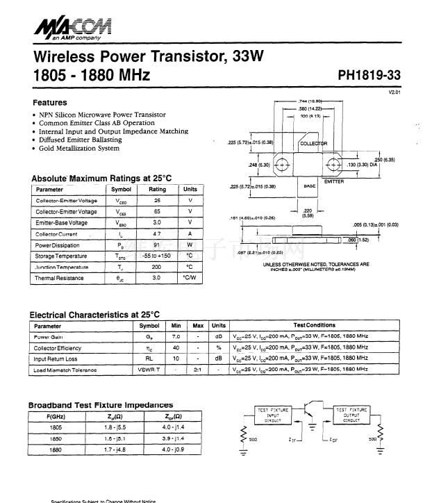
.744 (18.90)-1
NPN Silicon Microwave Power Transistor
Common Emitter Class AI3 Operation
Internal Input and Output Impedance Matching
Diffksed Emitter Ballasting
Gold Metallization System
225 (5.72)*.015 (0.38)
,
I
;48/6.30)
&&y&T
1
*\I
1
f
CqO(6.35)
Absolute鈥?Maximum Ratings at 25擄C
I
Parameter
Collector-EmitterVoltage
Collector-EmitterVoltage
Emitter-Base Voltage
CollectorCurrent
Power Dissipation
StorageTemperature
) JunctionTemperature
Thermal Resistance
I Sym~l
VCEO
VcE.s
Vem
I
鈥榗
PO
T c-Fe
)
T,
6
JC
I
Rating
25
65
3.0
1 Units
V
V
1
225(5.72)+.015
(0.38)
,181 (4.6O)zt.OlO
(0.25)
(5.59)
2.20 I--
.co5 (0.13)+.001 (0.03)
1
I
/
11
D6Ojl.52)
f
V
I
4.7
91
-55
to +150
I
*
w
鈥淐
I
t+
.087 (2.21)r.OlO (0.25)
1
200
3.0
I
鈥淐
鈥淐/W
I
UNLESS OTHERWISE NOTED, TOLERANCES ARE
INCHES
t.005鈥?(MILLIMETERS
t0.13MM)
Electrical Characteristics
Parameter
Power Gain
Collector Efficiency
Input Return Loss
r
at 25擄C
Symbol
GP
%
Min
7.0
40
Max
-
-
Units
dB
%
Test Conditions
I鈥?,=25 V, I,,=200 mA, PO,,=33 W, F=1805,1880 MHz
V,,=25 V, l,Q=200 mA, P,,,=33 W, F=l805,1880
V,,=25 V, I,,=200 mA, P,,,=33 W, F=l805,1880
MHz
MHz
RL
VSWR-T
10
-
-
2:l
dB
-
Load Mismatch Tolerance
V,,=25 V, I,,=200 mA, PO,,=33 W, F=1805,1880 MHz
Broadband Test Fixture impedances
I-
1805
~~
1850
I
1.8 - j5.5
I
4.0-j1.4
I
1.6 - j5.1
l.?-j4.8
3.9 - jl.4
4.0 -
j0.9
1880


 1
1
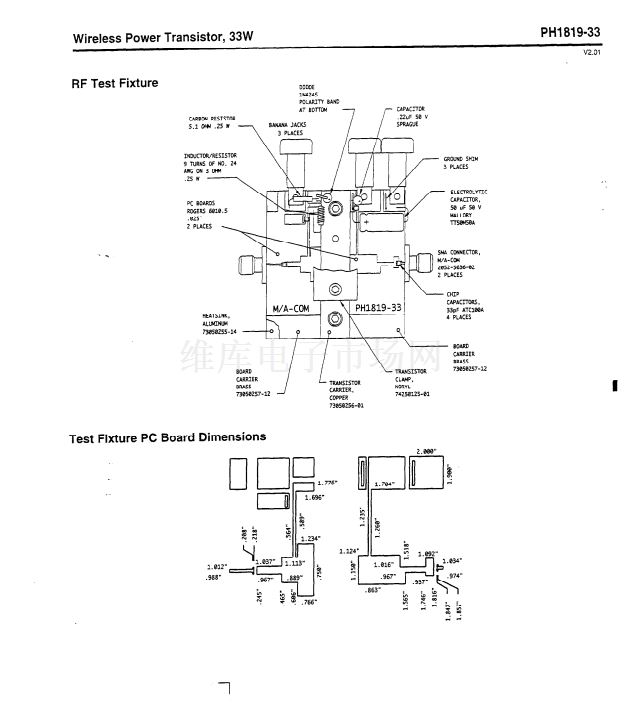 2
2
