*
an
AMP
company
,z==
i--s
=
-A=
=c
.--
---
-==
-
=
=
-
Wireless Bipolar Power Transistor, 1OW
1.78 - 1.90 GHz
Features
l
l
l
l
l
PH1819-10
v2.00
/
,744
:lE.SZ
+--,
5s:
.,4 22)
Designed for Cellular Base Station Applications
-30
dBc Typ 3rd IMD at 10 Watts PEP
Common Emitter Configuration
Internal Input Impedance Matching
Diffused Emitter BaIlasting
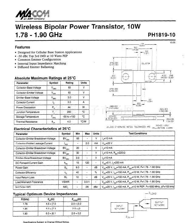
Absolute鈥榣blaximum
,
Ratings at 25擄C
I
/
I
Electrical Characteristics
Parameter
at 25擄C
Symbol
Min
Max
Units
Llli-ESS
CTiERWiSE
NOTED.
TOLERANCES
ARE
INCHES
(MILLIMETEPS
Z.COL
:.I3MM)
Test Conditions
Collector-Emitter Breakdown Voltage
Collector-Emitter Leakage Current
Collector-Emitter Breakdown Voltage
Collector-Emitter Breakdown Voltage
Emitter-Base Breakdown Voltage
DC Forward Current Gain
Power Gain
Collector Efficiency
input Return Loss
Load Mismatch Tolerance
3rd Order IMD
BVcE,
鈥楨S
BV,,,
BV,,
BVESO
hFE
GP
鈥業(yè)C
65
)
20
30
3.0
15
9.0
40
10
-
-
-
2.0
-
-
-
120
-
-
-
3.O:l
-28
V
) mA
V
V
V
-
dB
%
dB
-
dBc
I,=1 0 mA
) if,,=25 v
I,=1 0 mA
I,=1 0 mA. Q220R
IB=l 0 mA
V,,=5 V, I,=250 mA
V,,=25 V, I,,=1 00 mA, P,,flO
V,,=25
V, I,,=100
W, F=l.78 - 1.90 GHz
W, F=l.78 - 1.90 GHz
mA, P,,=lO
RL
VSWR
IMD,
V,,=25 V, I,,=1 00 mA, P,,,=lO W, F=l.78 - 1.90 GHz
V,,=25 V, I,,=1 00 mA, POUT=1W, F=l.78 - 1.90 GHz
0
V,,=25 V, lcO=l00 mA, P,,,=lO W PEP, F=l850 MHz, AF=lOO kHz
1
-
2 LlAD
Typical Optimum Device Impedances
F(GHz)
z,,w
Zo*o(Q)
1.78
1.85
4.5 + j7.0
5.0 + j7.3
2.5 + j0.2
2.5 + j0
2.6 + 0.2
pq-pzj
1.90
6.0 + j6.1
z:N
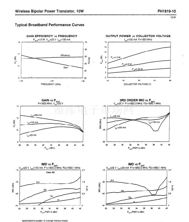
Specifications Subject to Change Without Notice.


 1
1
 2
2
 3
3
