=
=z
an
AMP
company
SC=
z
=
Radar Pulsed Power Transistor, 25W, 300~s Pulse, 10% Duty
PHI 214-25L
1.2 - 1.4 GHz
v2.00
Features
l
l
l
l
l
l
l
l
NPN Silicon Microwave Power Transistor
Common Base Configuration
Broadband Class C Operation
High Efficiency Interdigitated Geometry
Diffused Emitter Ballasting Resistors
Gold Metalization System
Internal Input Impedance Matching
Hermetic Metal/Ceramic Package
Absolute Maximum Ratings at 25擄C
Parameter
Collector-Emitter
Voltage
Symbol
V ES
V Em
Ic
P
TOT
TJ
T ST0
Rating
70
3.0
1.6
40
200
-65 to +200
Units
V
V
A
W
鈥淐
鈥淐
.3751.011
(9.33t.2))
1
Emitter-Base Voltage
Collector Current (Peak)
Total Power Dissipation
JunctionTemperature
StorageTemperature
/
UNLESS
OTHERWiSE
NOTED.
TOLERANCES
ARE
INCHES
鈥?OOS鈥?/div>
cMILLIMETERS
=,,3MM)
Electrical Characteristics
Parameter
Collector-Emitter
Collector-Emitter
Breakdown Voltage
Leakage Current
at 25擄C
Symbol
?Vcss
ICES
R -w(X)
PIN
GP
鈥榣C
Min
7.
Max
-
3.0
3.6
Units
V
mA
鈥淐NV
W
dB
%
dB
-
-
I,=25 mA
v,,=40
V,,=28
V,,=28
V,,=28
V,,=28
V,,=28
V,,=28
V,,=28
v
lest Conditions
Thermal Resistance
Input Power
Power Gain
Collector Efficiency
Input Return Loss
Load Mismatch Tolerance
Load Mismatch Stablility
V, PO,,=25 W, F=l.20,1.30,1.40
V, PO,,=25 W, Fzl.20,
GHz
-
9.5
50
6
-
-
2.8
-
-
-
3:l
1.5:1
1.30, 1.40 GHz
GHz
GHz
V, PO,,.=25 W, F=1.20,1.30,1.40
V, PO,,=25 W, F=1.20, 1.30,1.40
V, PO,=25 W, F=l.20,
RL
VSWR-T
VSWR-S
1.30, 1.40 GHz
V, PO,,=25 W, F=l.20,1.30,
1.40
GHz
GHz
V, PO,=25 W, F=1.20, 1.30,1.40
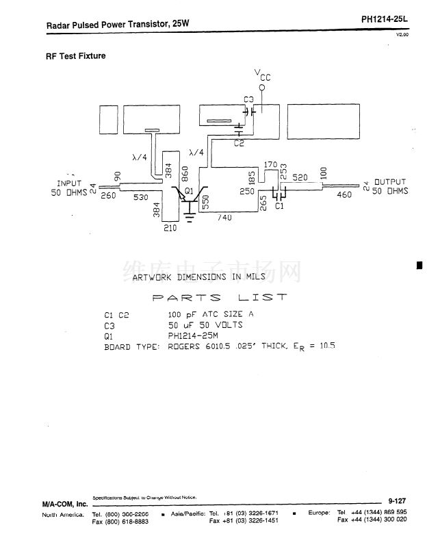
Broadband Test Fixture
ImtXdanCeS
F(GHz)
1.20
z,,(n)
2.1 - j4.5
Z,,(Q)
3.7+jO.9
I
3.6+jO.4
3.0 + j0.2
1
$TEqy--y$
-
M/A-COM,
n
1.30
1.40
I-
2.1 - j3.9
2.2 - j3.4
-
Inc.
Europe:
Tel. +44 (1344) 869 595
Fax +44 (1344) 300 020
Specifications Subject to Change Without Notice.
9-126
North America:
Tel. (800) 366-2266
Fax (800) 618-8883
s
Asia/Pacific:
Tel. ~81 (03) 3226-1671
Fax +81 (03) 3226-1451


 1
1
 2
2
