鈥?/div>
Spread Spectrum Clock Generator/Multiplier with
output selectable from 1x to 8x.
13MHz to 224MHz output with output enable.
13MHz to 30 MHz input frequency from crystal or
external clock signal.
Reduced EMI from Spread Spectrum Modulation,
with selectable modulation magnitude for Center
Spread, Down Spread or Asymmetric Spread.
TTL/CMOS compatible outputs.
3.3V Operating Voltage.
150 ps maximum cycle-to-cycle jitter.
Available in 16-Pin 150mil SSOP.
BLOCK DIAGRAM
REF
XIN/FIN
XOUT
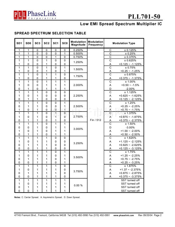
SC(0:3)
SD(0:1)
M(0:2)
XTAL
OSC
PLL
SST
Control
Logic
OE
FOUT
DIE PAD CONFIGURATION
69 mil
AVDD
GND
GND
XIN
1700, 2540
18
AVDD
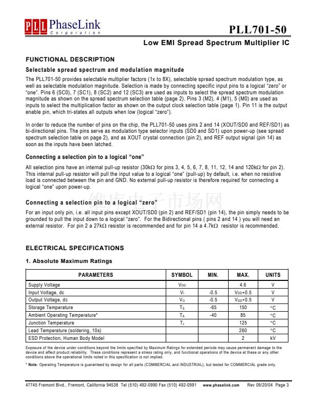
DESCRIPTION
The PLL701-50 is a low EMI Clock Generator and
Multiplier for high-speed digital systems. It uses
PhaseLink鈥檚 unique (Patent Pending) Spread
Spectrum Technology (SST) and permits different
levels of EMI reduction by selecting the amplitude of
the applied SST. The SST feature can be disabled.
The chip operates with input frequencies ranging from
13 to 30 MHz and provides 1x to 8x multiplication at
its output.
XOUT/SD0*^
23
22
21
(Optional)
20
(Optional)
19
GNDOSC
25
C501A
A2727
-27
17
16
15
14
13
12
AVDD
REF/SD1*^
VDD
VDD (optional)
VDD (optional)
SC3^
M2^
104 mil
M1^
M0^
28
29
30
10
OE^
OUTPUT CLOCK (FOUT) SELECTION
M2
M1
M0
FIN/XIN
(MHz)
Multiplier
FOUT
(MHz)
TESTB
SC0^
SC1^
33
34
35
1
4 5
6
8
7
FOUT
GNDBUF
0
0
0
0
1
1
1
1
0
0
1
1
0
0
1
1
0
1
0
1
0
1
0
1
13
13
14
13
20
17
15
13
~
~
~
~
~
~
~
~
28
28
30
28
30
30
30
28
X1
X2
X3
X4
X5
X6
X7
X8
13 ~ 28
26 ~ 56
42 ~ 90
52 ~ 112
100 ~ 150
102 ~ 180
105 ~ 210
104 ~ 224
SC2^
GND
GND
GND
Y
X
DIE SPECIFICATIONS
Name
Size
Reverse side
Pad dimensions
Thickness
Value
104 x 69 mil
GND
80 micron x 80 micron
10 mil
47745 Fremont Blvd., Fremont, California 94538 Tel (510) 492-0990 Fax (510) 492-0991
www.phaselink.com
Rev 09/20/04 Page 1


 1
1
 2
2
 3
3
 4
4
 5
5
 6
6
