鈥?/div>
Frequency range 50 ~ 120MHz.
Internal phase locked loop will allow spread spec-
trum modulation on reference clock to pass to the
outputs (up to 100kHz SST modulation).
Zero input - output delay.
Less than 700 ps device - device skew.
Less than 250 ps skew between outputs.
Less than 200 ps cycle - cycle jitter.
Output Enable function tri-state outputs.
3.3V operation.
Available in 8-Pin 150mil SOIC.
Remark
If REF clock is stopped for more than 10us after it has already been
provided to the chip, and after power-up, the output clocks will
disappear. In that instance, a full power-up reset is required in order
to reactivate the output clocks.
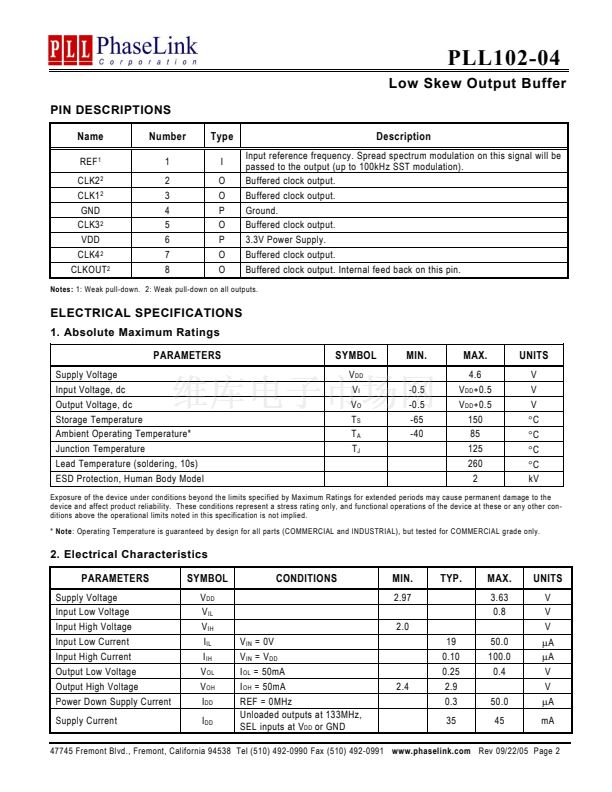
PIN CONFIGURATION
REF
CLK2
CLK1
GND
1
2
3
4
8
7
6
5
CLKOUT
CLK4
VDD
CLK3
PLL102-04
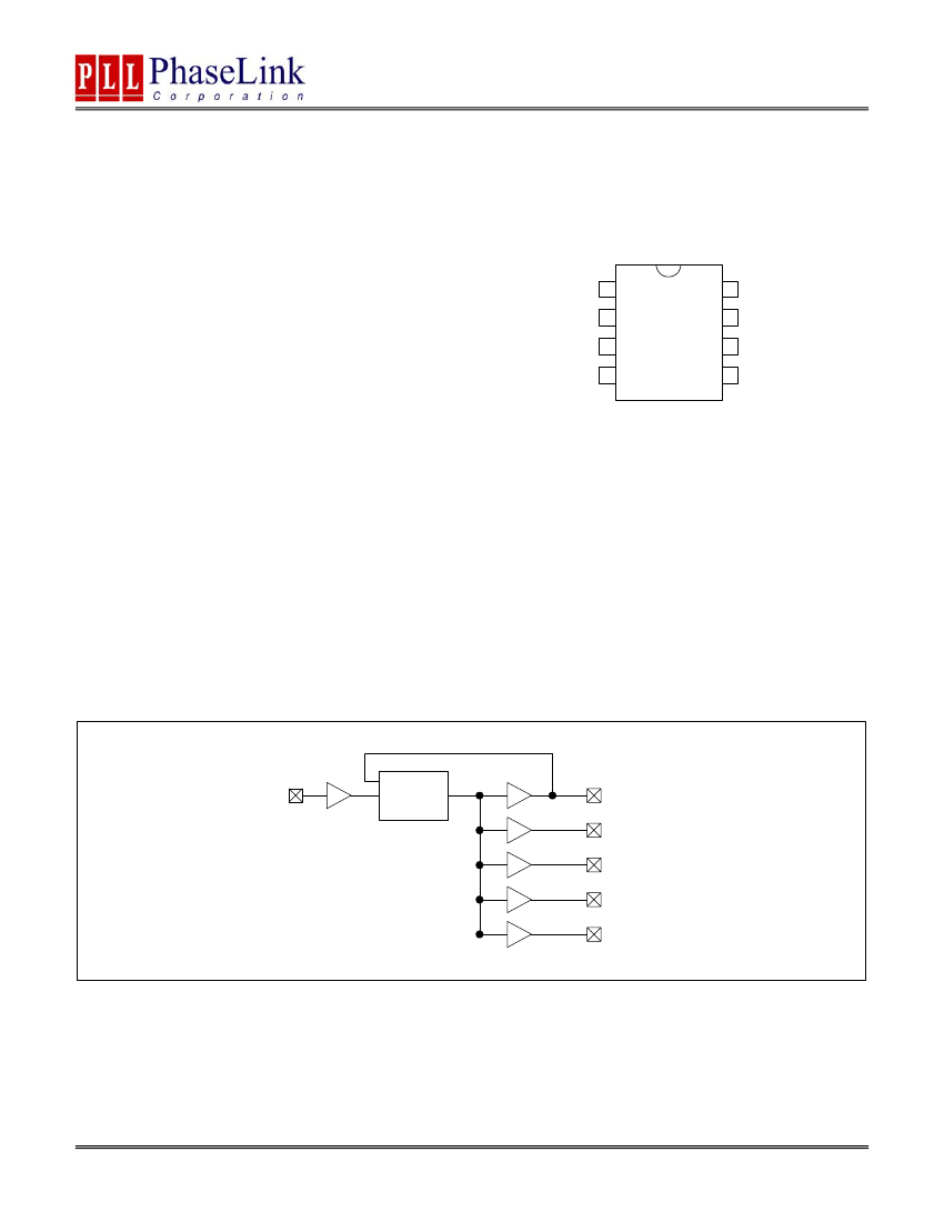
DESCRIPTION
The PLL102-04 is a high performance, low skew, low
jitter zero delay buffer designed to distribute high
speed clocks and is available in 8-pin SOIC package. It
has four outputs that are synchronized with the input.
The synchronization is established via CLKOUT feed
back to the input of the PLL. Since the skew between
the input and output is less than
鹵350
ps, the device
acts as a zero delay buffer.
BLOCK DIAGRAM
REF
PLL
CLKOUT
CLK1
CLK2
CLK3
CLK4
47745 Fremont Blvd., Fremont, California 94538 Tel (510) 492-0990 Fax (510) 492-0991
www.phaselink.com
Rev 09/22/05 Page 1


 1
1
 2
2
 3
3
 4
4
 5
5
 6
6
