鈥?/div>
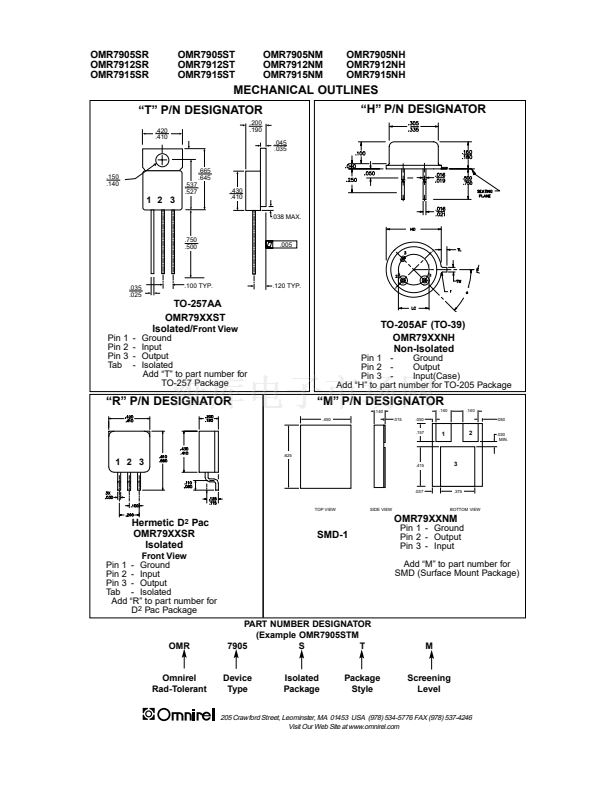
Isolated & Non-Isolated Hermetic Packages
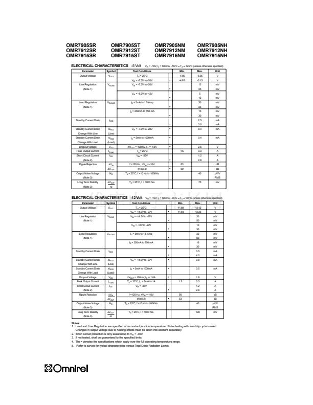
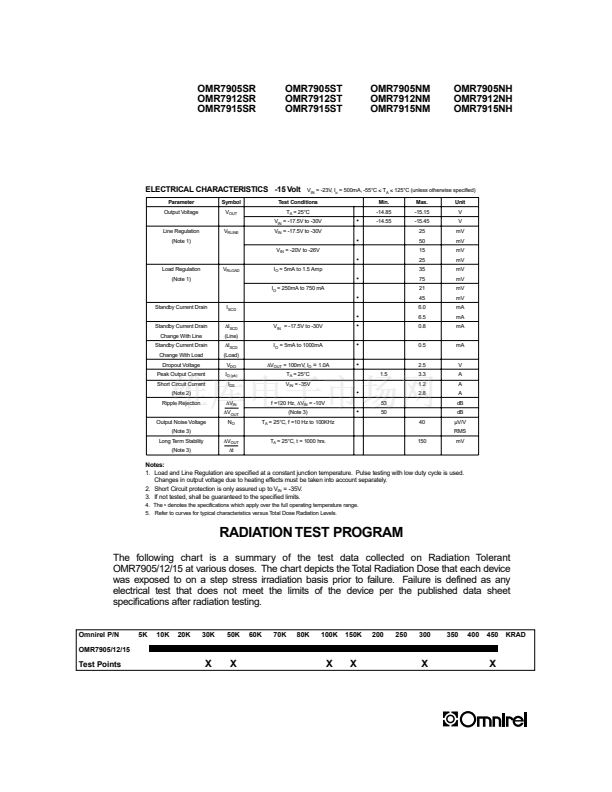
Output Voltages: -5V, -12V, -15V (Other Voltages Available)
Output Voltages Set Internally To 鹵1% or 鹵2%
Built-In Thermal Overload Protection
Short Circuit Current Limiting
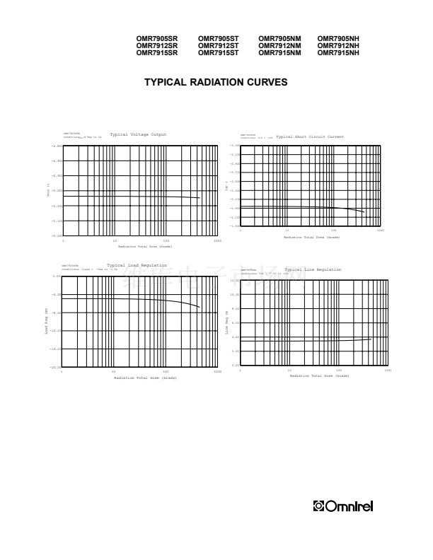
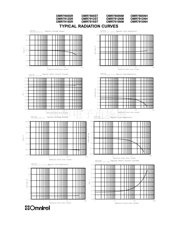
Radiation Tolerant up to 450 K Rad (Si)
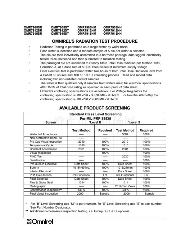
Available Hi-Rel Screened, Class B and Class S, MIL-STD-883
DESCRIPTION
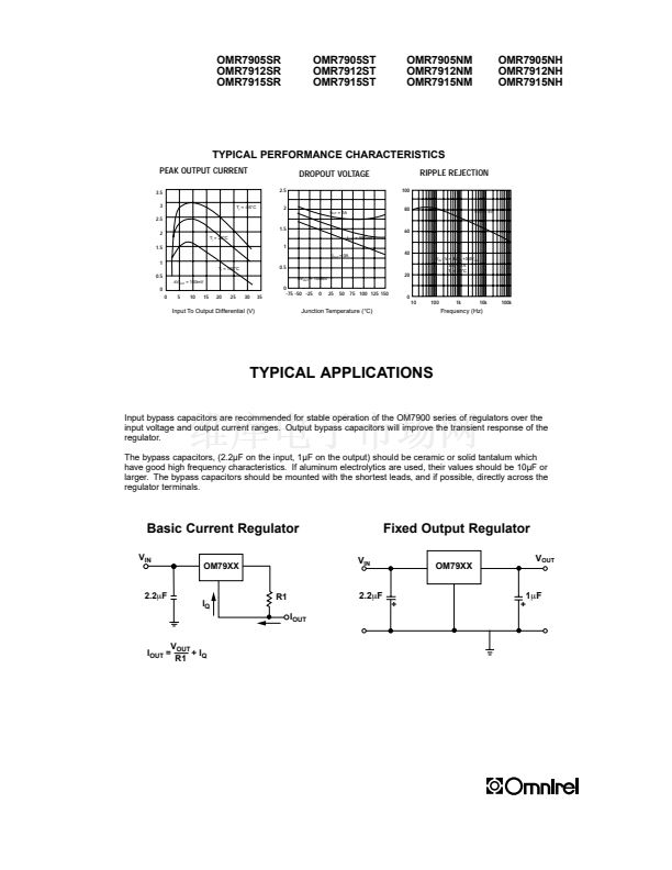
These three terminal negative regulators are supplied in a high density hermetically sealed
metal package and are available hi-rel screened. All protective features are designed into the
circuit, including thermal shutdown, current limiting and safe-area control. With heat sinking,
they can deliver over 1.5 amps of output current. These units feature internally trimmed output
voltages to 鹵1% or 2% of nominal voltage. Standard voltages are -5V, -12V, and
-15V. However, other voltages are available up to -24 volts. These devices are ideally suited
for Space applications where small size, high reliability, and radiation tolerance is required.
The high level of Radiation Tolerance of these devices makes them a desirable choice for LEO
and many MEO and GEO communication satellites. Radiation testing is performed on a single
wafer by wafer basis. Random die samples per wafer are selected, packaged and radiation
tested to qualify each individual semiconductor wafer-by-wafer.
ABSOLUTE MAXIMUM RATINGS
@ 25擄C
Input Voltage . . . . . . . . . . . . . . . . . . . . . . . . . . . . . . . . . . . . . . . . . . . . . . . . . . . . . . . . . . . . . . . . . . . . . . . . . -35 V
Operating Junction Temperature Range. . . . . . . . . . . . . . . . . . . . . . . . . . . . . . . . . . - 55擄C to + 150擄C
Storage Temperature Range. . . . . . . . . . . . . . . . . . . . . . . . . . . . . . . . . . . . . . . . . . . . . - 65擄C to + 150擄C
Power Dissipation: TO-205 . . . . . . . . . . . . . . . . . . . . . . . . . . . . . . . . . . . . . . . . . . . . . . . . . . . . . . . . . . . 1.1 W
TO-257/SMD/ D
2
Pac . . . . . . . . . . . . . . . . . . . . . . . . . . . . . . . . . . . . . . . . . . . . . . . . . . . . . . . . . . . . . . . . . 20 W
Lead Temperature (Soldering 10 seconds) . . . . . . . . . . . . . . . . . . . . . . . . . . . . . . . . . . . . . . . . . . . 300擄C
Surface Mount Package Soldering Temperature . . . . . . . . . . . . . . . . . . . . . . . . . . . . . . . . . . . . . . 250擄C
Thermal Resistance, Junction to Case:
TO-205 . . . . . . . . . . . . . . . . . . . . . . . . . . . . . . . . . . . . . . . . . . . . . . . . . . . . . . . . . . . . . . . . . . . . . . . 17擄C/W
TO-257(Isolated), D
2
Pac (Isolated) . . . . . . . . . . . . . . . . . . . . . . . . . . . . . . . . . . . . . . . . . . 4.2擄C/W
SMD-1 . . . . . . . . . . . . . . . . . . . . . . . . . . . . . . . . . . . . . . . . . . . . . . . . . . . . . . . . . . . . . . . . . . . . . . . 3.5擄C/W
Thermal Resistance, (Junction Ambient):
TO-205 . . . . . . . . . . . . . . . . . . . . . . . . . . . . . . . . . . . . . . . . . . . . . . . . . . . . . . . . . . . . . . . . . . . . . . . 90擄C/W
TO-257(Isolated), D
2
Pac (Isolated) SMD-1 . . . . . . . . . . . . . . . . . . . . . . . . . . . . . . . . . . . 42擄C/W
Maximum Output Current: TO-205. . . . . . . . . . . . . . . . . . . . . . . . . . . . . . . . . . . . . . . . . . . . . . . . . . . . 0.5 A
Case-All Others . . . . . . . . . . . . . . . . . . . . . . . . . . . . . . . . . . . . . . . . . . . . . . . . . . . . . . . . . . . . . . . . . . 3.3A
Radiation Tolerant - Total Dose . . . . . . . . . . . . . . . . . . . . . . . . . . . . . . . . . . . . . . . . . . . . . . 300 K Rad (Si)
0 04 R1
Supersedes 9 12 R0


 1
1
 2
2
 3
3
 4
4
 5
5
 6
6
 7
7
 8
8
