NZT560/NZT560A
NZT560/NZT560A
NPN Low Saturation Transistor
鈥?These devices are designed with high current gain and low saturation
voltage with collector currents up to 3A continuous.
3
2
1
4
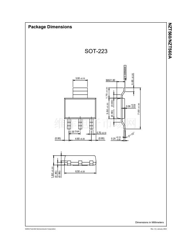
SOT-223
1. Base 2. Collector 3. Emitter
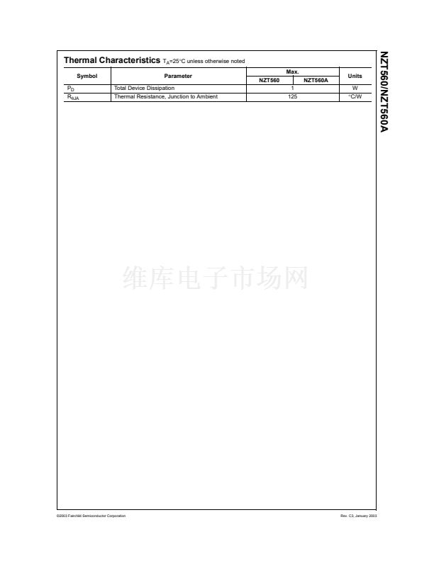
Absolute Maximum Ratings*
T
A
=25擄C unless otherwise noted
Symbol
V
CEO
V
CBO
V
EBO
I
C
T
J
, T
STG
Collector-Emitter Voltage
Collector-Base Voltage
Emitter-Base Voltage
Collector Current
- Continuous
Operating and Storage Junction Temperature Range
Parameter
NZT560/NZT560A
60
80
5
3
- 55 ~ +150
Units
V
V
V
A
擄C
* These ratings are limiting values above which the serviceability of any semiconductor device may be impaired.
NOTES:
1) These ratings are based on a maximum junction temperature of 150擄C.
2) These are steady state limits. The factory should be consulted on applications involving pulsed or low duty cycle operations.
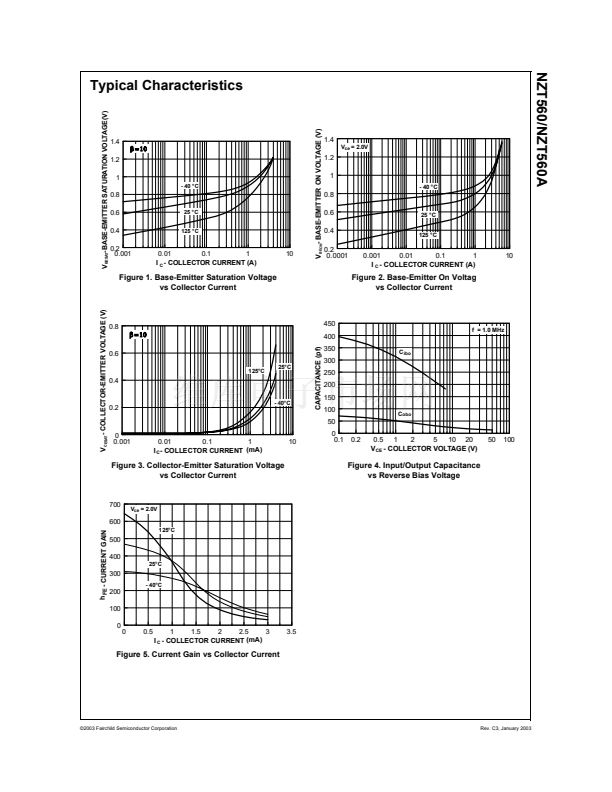
Electrical Characteristics
T
A
=25擄C unless otherwise noted
Symbol
Off Characteristics
BV
CEO
BV
CBO
BV
EBO
I
CBO
I
EBO
h
FE
Parameter
I
C
= 10mA
I
C
= 100碌A(chǔ)
I
E
= 100碌A(chǔ)
V
CB
= 30V
V
CB
= 30V, T
A
= 100擄C
V
EB
= 4V
I
C
= 100mA, V
CE
= 2V
I
C
= 500mA, V
CE
= 2V
I
C
= 1A, V
CE
= 2V
I
C
= 3A, V
CE
= 2V
V
CE
(sat)
Collector-Emitter Saturation Voltage
I
C
= 1A, I
B
= 100mA
I
C
= 3A, I
B
= 300mA
I
C
= 1A, I
B
= 100mA
I
C
= 1A, V
CE
= 2V
V
CB
= 10V, I
E
= 0, f = 1MHz
I
C
= 100mA, V
CE
= 5V, f = 100MHz
75
NZT560
NZT560A
70
100
250
80
25
Test Conditions
Min.
60
80
5
100
10
100
Typ.
Max.
Units
V
V
V
V
nA
碌A(chǔ)
nA
Collector-Emitter Breakdown Voltage
Collector-Base Breakdown Voltage
Emitter-Base Breakdown Voltage
Collector Cutoff Current
Emitter Cutoff Current
DC Current Gain
On Characteristics *
NZT560
NZT560A
300
550
300
450
400
1.25
1
30
mV
mV
mV
V
V
pF
MHz
V
BE
(sat)
V
BE
(on)
C
obo
Base-Emitter Saturation Voltage
Base-Emitter On Voltage
Output Capacitance
Small Signal Characteristics
Transition Frequency
f
T
* Pulse Test: Pulse Width
鈮?/div>
300碌s, Duty Cycle
鈮?/div>
2.0%
漏2003 Fairchild Semiconductor Corporation
Rev. C3, January 2003


 1
1
 2
2
 3
3
 4
4
 5
5
