Lead Solder Temperature 鈭?/div>
Maximum 10 Seconds Duration
Symbol
P
pk
I
PP
T
J
, T
stg
T
L
Value
300
17
鈭?5 to
+150
260
Unit
W
A
6101
A
Y
W
= Device Code
= Assembly Location
= Year
= Work Week
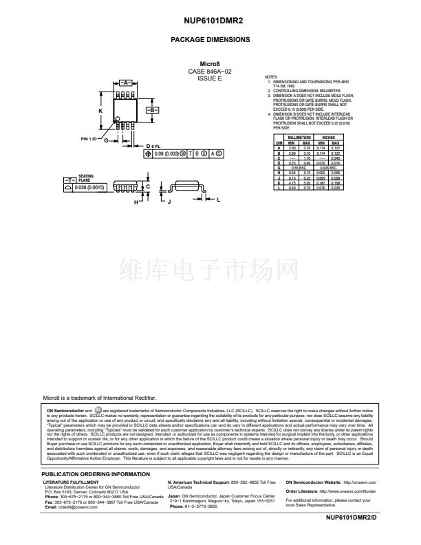
PIN ASSIGNMENT
擄C
擄C
Source
Source
Source
Gate
1
2
3
4
8
7
6
5
Drain
Drain
Drain
Drain
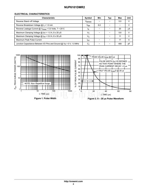
1. Non鈭抮epetitive current pulse 8 x 20
mS
exponential decay waveform
Top View
ORDERING INFORMATION
Device
NUP6101DMR2
Package
Micro8
Shipping
鈥?/div>
4000 Tape & Reel
鈥燜or information on tape and reel specifications,
including part orientation and tape sizes, please
refer to our Tape and Reel Packaging Specification
Brochure, BRD8011/D.
漏
Semiconductor Components Industries, LLC, 2004
1
March, 2004 鈭?Rev. 1
Publication Order Number:
NUP6101DMR2/D


 1
1
 2
2
 3
3
 4
4
