鈥?/div>
Cell Phone Vibrators
1
Q1
2
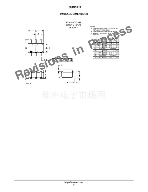
419B
Unit
Vdc
Vdc
mAd
c
Vdc
3
MAXIMUM RATINGS
(T
A
= 25擄C unless otherwise noted)
Rating
Collector-Base Voltage
Emitter-Base Voltage
Collector-Current - Continuous
Diode Reverse Voltage
Symbol
V
CBO
V
EBO
I
C
V
R
Value
15
5.0
100
12
MARKING
DIAGRAMS
5
4
J2 D
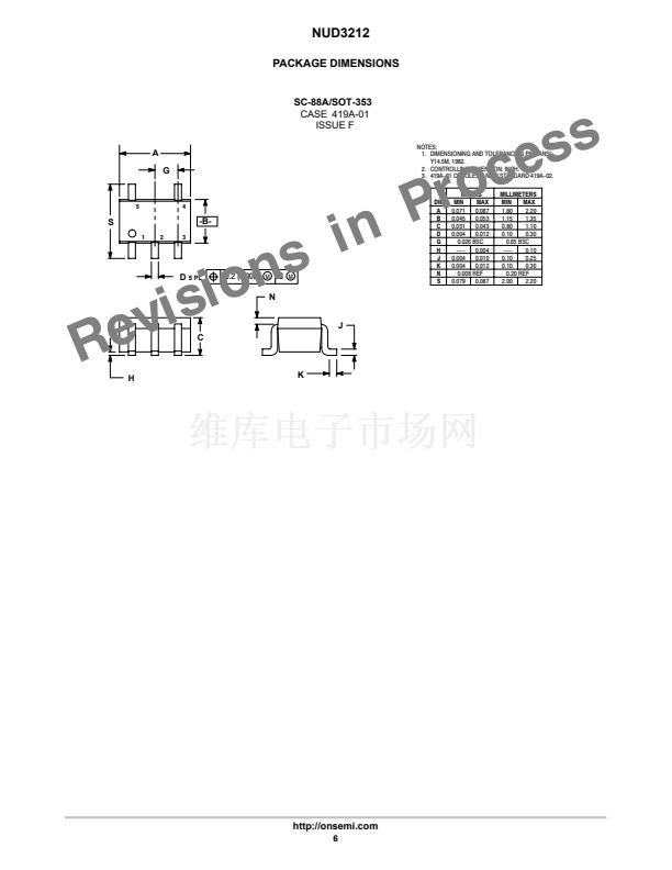
SC-88A (SOT-353)
CASE 419A
Style 8
1
2
3
THERMAL CHARACTERISTICS
Characteristic
Total Device Dissipation
Thermal Resistance Junction to Ambient
Junction and Storage Temperature
Symbol
P
D
R
qJA
T
J
, T
stg
Max
150
833
-55 to 150
Unit
mW
擄C/W
擄C
6
J2 D
SC-88 (SOT-363)
CASE 419B
Style 25
1
This document contains information on a product under development. ON Semiconductor
reserves the right to change or discontinue this product without notice.
J2 = Specific Device Code
D = Date Code
ORDERING INFORMATION
Device
NUD3212W5T1
NUD3212DWT1
Package
SC-88A
SC-88
Shipping
3000 Tape & Reel
3000 Tape & Reel
漏
Semiconductor Components Industries, LLC, 2003
1
June, 2003 - Rev. P0
Publication Order Number:
NUD3212/D


 1
1
 2
2
 3
3
 4
4
 5
5
 6
6
 7
7
 8
8
