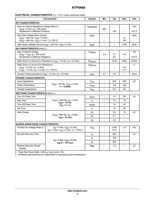
RDS(on) = 2400 m鈩?/div>
N鈥揅hannel
D
Typical Applications
G
S
MAXIMUM RATINGS
(TC = 25擄C unless otherwise noted)
Rating
Drain鈥揝ource Voltage
Drain鈥揋ate Voltage (RGS = 1.0 M鈩?
Gate鈥揝ource Voltage
鈥?Continuous
鈥?Non鈥揜epetitive (tp
v10
ms)
Drain 鈥?Continuous @ TA 25擄C
鈥?Continuous @ TA 100擄C
鈥?Single Pulse (tp
v10
碌s)
Total Power Dissipation @ TA 25擄C
Derate above 25擄C
Total Power Dissipation @ TA 25擄C
(Note 1.)
Operating and Storage
Temperature Range
Single Drain鈥搕o鈥揝ource Avalanche
Energy 鈥?Starting TJ = 25擄C
(VDD = 100 V, VGS = 10 Vdc,
IL(pk) = 5 A, L = 10 mH, VDS = 600
Vdc, RG = 25
鈩?
Thermal Resistance
鈥?Junction鈥搕o鈥揅ase
鈥?Junction鈥搕o鈥揂mbient
Maximum Lead Temperature for
Soldering Purposes, 1/8鈥?from case
for 10 seconds
Symbol
VDSS
VDGR
VGS
VGS
ID
ID
IDM
PD
Value
600
600
"20
"40
5
3.8
17.5
96
0.77
1.75
鈥?5 to
+150
80
Adc
Apk
Watts
W/擄C
Watts
擄C
mJ
1
Unit
Vdc
Vdc
Vdc
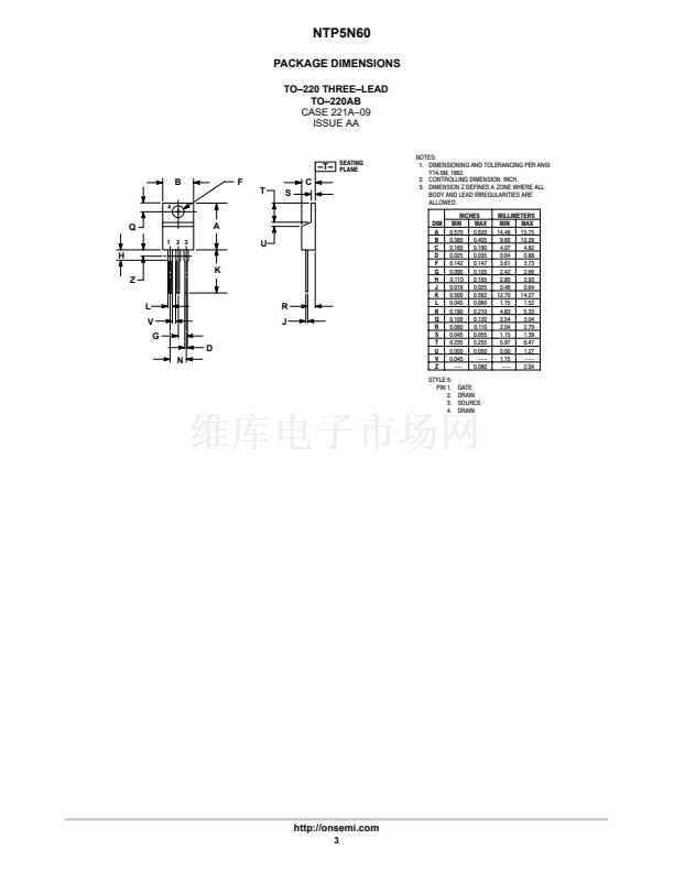
MARKING DIAGRAMS
AND PIN ASSIGNMENTS
Drain
4
TO鈥?20AB
CASE 221A
STYLE 5
NTP5N60
LLYWW
Gate
Source
2
3
NTP5N60
LL
Y
WW
Drain
= Device Code
= Location Code
= Year
= Work Week
TJ, Tstg
EAS
ORDERING INFORMATION
擄C/W
R
胃JC
R
胃JA
TL
1.3
62.5
260
擄C
Device
NTP5N60
Package
TO鈥?20AB
Shipping
50 Units/Rail
Preferred
devices are recommended choices for future use
and best overall value.
1. Repetitive rating; pulse width limited by maximum junction temperature.
This document contains information on a product under development. ON Semiconductor
reserves the right to change or discontinue this product without notice.
漏
Semiconductor Components Industries, LLC, 2000
1
November, 2000 鈥?Rev. 0
Publication Order Number:
NTP5N60/D


 1
1
 2
2
 3
3
 4
4
