Thermal Resistance 鈥?/div>
Junction鈥搕o鈥揂mbient (Note 3.)
Total Power Dissipation @ T
A
= 25擄C
Continuous Drain Current @ T
A
= 25擄C
Continuous Drain Current @ T
A
= 100擄C
Pulsed Drain Current (Note 4.)
Operating and Storage
Temperature Range
Single Pulse Drain鈥搕o鈥揝ource Avalanche
Energy 鈥?Starting T
J
= 25擄C (V
DD
=
鈥?0 Vdc, V
GS
= 鈥?.5 Vdc, Peak I
L
=
鈥?.0 Apk, L = 28 mH, R
G
= 25
鈩?
Maximum Lead Temperature for Soldering
Purposes, 1/8鈥?from case for 10 seconds
Symbol
V
DSS
V
GS
R
胃JA
P
D
I
D
I
D
I
DM
R
胃JA
P
D
I
D
I
D
I
DM
R
胃JA
P
D
I
D
I
D
I
DM
T
J
, T
stg
E
AS
Value
鈥?0
"10
175
0.71
鈥?.3
鈥?.45
鈥?.0
105
1.19
鈥?.97
鈥?.88
鈥?2
62.5
2.0
鈥?.85
鈥?.43
鈥?5
鈥?5 to
+150
350
Unit
V
V
擄C/W
W
A
A
A
擄C/W
W
A
A
A
擄C/W
W
A
A
A
擄C
mJ
A
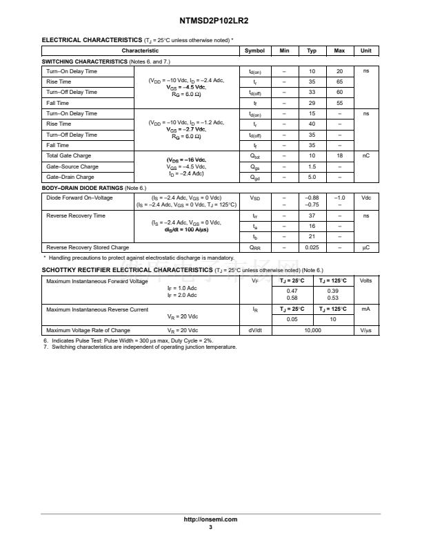
8
1
SO鈥?
CASE 751
STYLE 18
A
S
G
1
2
3
4
8
7
6
5
C
C
D
D
TOP VIEW
MARKING DIAGRAM
& PIN ASSIGNMENTS
Anode
Anode
Source
Gate
1
2
3
4
(Top View)
E2P102L= Device Code
L
= Assembly Location
Y
= Year
WW
= Work Week
E2P102L
LYWW
8
7
6
5
Cathode
Cathode
Drain
Drain
T
L
260
擄C
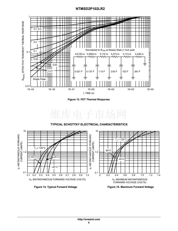
1. Minimum FR鈥? or G鈥?0 PCB, Steady State.
2. Mounted onto a 2鈥?square FR鈥? Board (1鈥?sq. 2 oz Cu 0.06鈥?thick single
sided), Steady State.
3. Mounted onto a 2鈥?square FR鈥? Board (1鈥?sq. 2 oz Cu 0.06鈥?thick single
sided), t
鈮?/div>
10 seconds.
4. Pulse Test: Pulse Width = 300
ms,
Duty Cycle = 2%.
This document contains information on a product under development. ON Semiconductor
reserves the right to change or discontinue this product without notice.
ORDERING INFORMATION
Device
NTMSD2P102LR2
Package
SO鈥?
Shipping
2500/Tape & Reel
漏
Semiconductor Components Industries, LLC, 2000
1
November, 2000 鈥?Rev. 0
Publication Order Number:
NTMSD2P102LR2/D


 1
1
 2
2
 3
3
 4
4
 5
5
 6
6
 7
7
 8
8
 9
9
 10
10
 11
11
 12
12
