鈥?/div>
DC鈭扗C Converters
MAXIMUM RATINGS
(T
J
= 25擄C unless otherwise noted)
Rating
Drain鈭抰o鈭扴ource Voltage
Gate鈭抰o鈭扴ource Voltage
Continuous Drain
Current (N t 1)
C
t (Note
Steady
State
t
v10
s
Power Dissi ation
Dissipation
(Note 1)
Steady
State
t
v10
s
Continuous Drain
Current
C rrent (Note 2)
Power Dissi ation
Dissipation
(Note 2)
Pulsed Drain Current
Steady
y
State
T
A
= 25擄C
T
A
= 85擄C
T
A
= 25擄C
P
D
T
A
= 25擄C
25 C
2.5
T
A
= 25擄C
T
A
= 85擄C
T
A
= 25擄C
t
p
= 10
ms
P
D
I
DM
T
J
, T
stg
I
S
E
AS
I
D
11
8.0
0.93
56
鈭?5 to
150
3.0
880
W
A
擄C
A
mJ
A
Symbol
V
DSS
V
GS
I
D
Value
30
$20
15
11
18
1.67
W
Unit
V
V
A
D
G
S
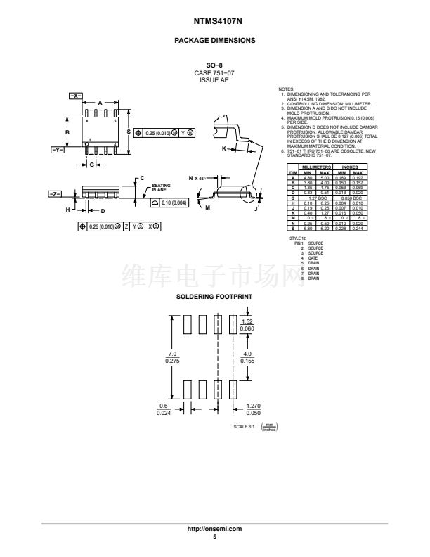
MARKING DIAGRAM/
PIN ASSIGNMENT
1
8
1
SO鈭?
CASE 751
STYLE 12
Source
Source
Source
Gate
4107N
ALYW
(Top View)
8
Drain
Drain
Drain
Drain
Operating Junction and Storage Temperature
Continuous Source Current (Body Diode)
Single Pulse Drain鈭抰o鈭扴ource Avalanche
Energy (V
DD
= 30 V, V
GS
= 10 V, I
PK
= 42 A,
L = 1 mH, R
G
= 25
W)
Lead Temperature for Soldering Purposes
(1/8鈥?from case for 10 s)
T
L
260
擄C
4107N
A
L
Y
W
= Specific Device Code
= Assembly Location
= Wafer Lot
= Year
= Work Week
THERMAL RESISTANCE RATINGS
Rating
Junction鈭抰o鈭扐mbient 鈭?Steady State (Note 1)
Junction鈭抰o鈭扐mbient 鈭?t
v
10 s (Note 1)
Junction鈭抰o鈭扐mbient 鈭?Steady State (Note 2)
Symbol
R
qJA
R
qJA
R
qJA
Max
75
50
135
Unit
擄C/W
ORDERING INFORMATION
Device
NTMS4107NR2
Package
SO鈭?
Shipping鈥?/div>
2500/Tape & Reel
Maximum ratings are those values beyond which device damage can occur.
Maximum ratings applied to the device are individual stress limit values (not
normal operating conditions) and are not valid simultaneously. If these limits are
exceeded, device functional operation is not implied, damage may occur and
reliability may be affected.
1. Surface鈭抦ounted on FR4 board using 1鈥?sq. pad size
(Cu area = 1.127鈥?sq. [1 oz] including traces).
2. Surface鈭抦ounted on FR4 board using the minimum recommended pad size
(Cu area = 0.412鈥?sq.).
鈥燜or information on tape and reel specifications,
including part orientation and tape sizes, please
refer to our Tape and Reel Packaging Specifications
Brochure, BRD8011/D.
漏
Semiconductor Components Industries, LLC, 2005
1
March, 2005 鈭?Rev. 1
Publication Order Number:
NTMS4107N/D


 1
1
 2
2
 3
3
 4
4
 5
5
 6
6
