鈥?/div>
Buck and Boost DC鈭扗C Converters
MAXIMUM RATINGS
(T
J
= 25擄C unless otherwise noted)
Rating
Drain鈭抰o鈭扴ource Voltage
Gate鈭抰o鈭扴ource Voltage
Continuous Drain
Current (Note 1)
Power Dissi ation
Dissipation
(Note 1)
Pulsed Drain Current
Steady
State
Steady
State
T
A
= 25擄C
T
A
= 85擄C
T
A
= 25擄C
T
A
= 85擄C
Symbol
V
DSS
V
GS
I
D
Value
鈭?0
"12
鈭?.1
鈭?.5
1.1
P
D
I
DM
T
J
, T
stg
I
S
T
L
0.6
鈭?.0
鈭?5 to
150
鈭?.1
260
W
A
擄C
A
擄C
A
Unit
V
V
G
1
200 mW @ 鈭?.5 V
S
1
S
2
G
2
D
1
P鈭扖hannel MOSFET
D
2
P鈭扖hannel MOSFET
tp = 10
ms
ChipFET
CASE 1206A
Style 2
Operating Junction and Storage Temperature
Source Current (Body Diode)
Lead Temperature for Soldering Purposes
(1/8鈥?from case for 10 s)
PIN
CONNECTIONS
D
1
D
1
8
7
6
5
1
2
3
4
MARKING
DIAGRAM
1
2
3
4
C4
8
7
6
5
S
1
G
1
S
2
G
2
THERMAL RESISTANCE RATINGS
Rating
Junction鈭抰o鈭扐mbient 鈭?Steady State (Note 1)
Symbol
R
qJA
Value
110
Unit
擄C/W
D
2
D
2
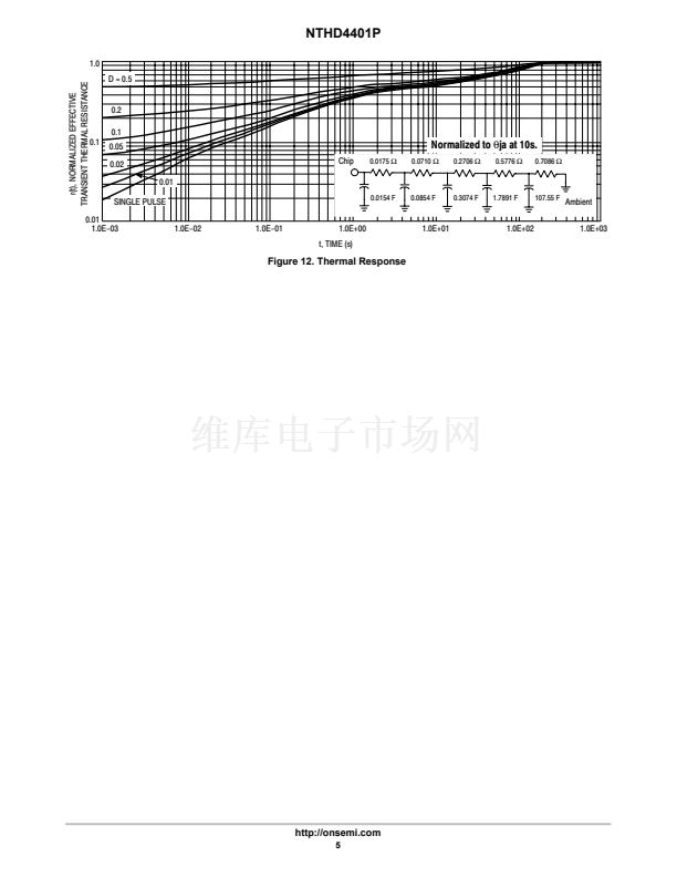
1. Surface鈭抦ounted on FR4 board using 1鈥?sq. pad size (Cu. area = 1.127鈥?sq.
[1 oz.] including traces).
C4 = Specific Device Code
ORDERING INFORMATION
Device
NTHD4401PT1
NTHD4401PT1G
Package
ChipFET
ChipFET
(Pb鈭扚ree)
Shipping
鈥?/div>
3000/Tape & Reel
3000/Tape & Reel
鈥燜or information on tape and reel specifications,
including part orientation and tape sizes, please
refer to our Tape and Reel Packaging Specifications
Brochure, BRD8011/D.
漏
Semiconductor Components Industries, LLC, 2003
1
October, 2003 鈭?Rev. 2
Publication Order Number:
NTHD4401P/D


 1
1
 2
2
 3
3
 4
4
 5
5
 6
6
 7
7
 8
8
