SaRonix
Crystal Clock Oscillator
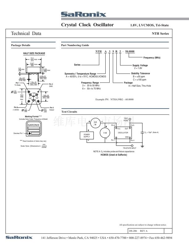
Technical Data
Frequency Range:
Frequency Stability:
20 MHz to 70 MHz
鹵50 or 鹵100 ppm over all conditions: calibration tolerance,
operating temperature, input voltage change, load change,
aging, shock and vibration.
1.8V, LVCMOS, Tri-State
NTH Series
Temperature Range:
Operating:
Storage:
Supply Voltage:
Recommended Operating:
Supply Current:
ACTUAL SIZE
0 to +70擄C
-55 to +125擄C
1.8V 鹵5%
6mA max 20 to 50 MHz, output enabled
10mA max 50+ to 70MHz, output enabled
10碌A(chǔ) max 20 to 70MHz, output disabled
Description
A 1.8V LVDS, crystal controlled, low
current, low jitter oscillator with precise
rise and fall times demanded in network-
ing applications, such as Gigabit Ethernet
and Fibre Channel. The Tri-State func-
tion enables the output to go high im-
pedance. Device is packaged in an 8-
pin DIP compatible resistance welded,
all metal grounded case, to reduce EMI.
Applications & Features
鈥?/div>
鈥?/div>
鈥?/div>
鈥?/div>
鈥?/div>
鈥?/div>
Fibre Channel
Gigabit Ethernet
32 Bit Microprocessors
Tri-State output standard
LVCMOS / HCMOS compatible
Grounded, all metal half size case
Output Drive:
Symmetry:
Rise and Fall Times:
Logic 0:
Logic 1:
Load:
Period Jitter RMS:
Mechanical:
Shock:
Solderability:
Terminal Strength:
Vibration:
Solvent Resistance:
Resistance to Soldering Heat:
Environmental:
Gross Leak Test:
Fine Leak Test:
Thermal Shock:
Moisture Resistance:
MIL-STD-883,
MIL-STD-883,
MIL-STD-883,
MIL-STD-883,
MIL-STD-202,
MIL-STD-202,
Method 2002, Condition B
Method 2003
Method 2004, Conditions B2
Method 2007, Condition A
Method 215
Method 210, Condition A, B or C
45/55% max @ 50% V
DD
2.5ns max
10% V
DD
max
90% V
DD
min
15 pF max
8ps max
MIL-STD-883,
MIL-STD-883,
MIL-STD-883,
MIL-STD-883,
Method
Method
Method
Method
1014, Condition C
1014, Condition A2
1011, Condition A
1004
Output Waveform
CMOS
T
r
1 Level
80% V
DD
50% V
DD
20% V
DD
0 Level
SYMMETRY
GND
T
f
V
DD
Tri-State
Logic Table:
Pin 1 Input
Logic 1 or NC
Logic 0 or GND
Control Characteristics:
Output:
Output:
Internal Pullup Resistance:
Control Input:
Control Input:
Pin 5 Output
Oscillation
High Impedance
Oscillation @ V
IN
, 2.2V min
High Impedance @ V
IN
, 0.8V max
50K鈩?min
Disable Output Delay: 100ns max
Enable Output Delay: 10ms max
DS-206
REV A
SaRonix
141 Jefferson Drive 鈥?Menlo Park, CA 94303 鈥?USA 鈥?650-470-7700 鈥?800-227-8974 鈥?Fax 650-462-9894
NTH+1.8V相關(guān)型號(hào)PDF文件下載


 1
1
 2
2
