NTE99
Silicon NPN Transistor
Darlington
w
/Base鈥揈mitter Speed鈥搖p Diode
Description:
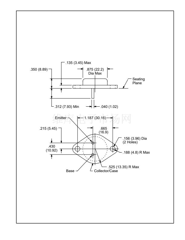
The NTE99 is a silicon NPN Darlington transistor in a TO3 type package designed for high鈥搗oltage,
high鈥搒peed, power switching in inductive circuits where fall time is critical. This device is particularly
suited for line鈥搊perated switchmode applications.
Applications:
D
Switching Regulators
D
Motor Controls
D
Inverters
D
Solenoid and Relay Drivers
Features:
D
Fast Turn鈥揙ff Times:
1.0碌s (max) Inductive Crossover Time 鈥?20 Amps
2.5碌s (max) Inductive Storage Time 鈥?20 Amps
D
Operating Temperature Range: 鈥?5擄 to +200擄C
Absolute Maximum Ratings:
Collector鈥揈mitter Voltage, V
CEO
. . . . . . . . . . . . . . . . . . . . . . . . . . . . . . . . . . . . . . . . . . . . . . . . . . . . . 400V
Collector鈥揈mitter Voltage, V
CEV
. . . . . . . . . . . . . . . . . . . . . . . . . . . . . . . . . . . . . . . . . . . . . . . . . . . . . 600V
Emitter鈥揃ase Voltage, V
EB
. . . . . . . . . . . . . . . . . . . . . . . . . . . . . . . . . . . . . . . . . . . . . . . . . . . . . . . . . . . 8V
Collector Current, I
C
Continuous . . . . . . . . . . . . . . . . . . . . . . . . . . . . . . . . . . . . . . . . . . . . . . . . . . . . . . . . . . . . . . . . . . 50A
Peak (Note 1) . . . . . . . . . . . . . . . . . . . . . . . . . . . . . . . . . . . . . . . . . . . . . . . . . . . . . . . . . . . . . . . . 75A
Base Current, I
B
Continuous . . . . . . . . . . . . . . . . . . . . . . . . . . . . . . . . . . . . . . . . . . . . . . . . . . . . . . . . . . . . . . . . . . 10A
Peak (Note 1) . . . . . . . . . . . . . . . . . . . . . . . . . . . . . . . . . . . . . . . . . . . . . . . . . . . . . . . . . . . . . . . . 15A
Total Power Dissipation, P
D
T
C
= +25擄C . . . . . . . . . . . . . . . . . . . . . . . . . . . . . . . . . . . . . . . . . . . . . . . . . . . . . . . . . . . . . . . . 250W
Derate Above 25擄C . . . . . . . . . . . . . . . . . . . . . . . . . . . . . . . . . . . . . . . . . . . . . . . . . . . . . . 1.43W/擄C
T
C
= +100擄C . . . . . . . . . . . . . . . . . . . . . . . . . . . . . . . . . . . . . . . . . . . . . . . . . . . . . . . . . . . . . . . 143W
Operating Junction Temperature Range, T
J
. . . . . . . . . . . . . . . . . . . . . . . . . . . . . . . . . . 鈥?5擄 to +200擄C
Storage Temperature Range, T
stg
. . . . . . . . . . . . . . . . . . . . . . . . . . . . . . . . . . . . . . . . . . 鈥?5擄 to +200擄C
Thermal Resistance, Junction鈥搕o鈥揅ase, R
thJC
. . . . . . . . . . . . . . . . . . . . . . . . . . . . . . . . . . . . . 0.7擄C/W
Maximum Lead Temperature (During Soldering, 1/8鈥?from case for 5sec), T
L
. . . . . . . . . . . . +275擄C
Note 1. Pulse Test: Pulse Width = 5ms, Duty Cycle
next


 1
1
 2
2
 3
3
