NTE975 & NTE975SM
Integrated Circuit
Operational Amplifier
Description:
The NTE975 and NTE975SM are general purpose operational amplifiers built on a single chip. The
resulting close match and tight thermal coupling gives low offsets and temperature drift as well as fast
recovery from thermal transients.
The unity鈥揼ain compensation specified makes the circuit stable for all feedback configurations, even
with capacitive loads. However, it is possible to optimize compensation for the best high frequency
performance at any gain. As a comparator, the output can be clamped at any desired level to make
it compatible with logic circuits.
Features:
D
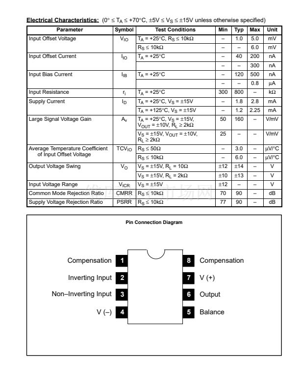
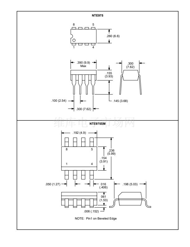
Available in 8鈥揕ead Mini DIP (NTE975) and Surface Mount, SOIC鈥? (NTE975SM)
D
Frequency Compensation with a Single 30pF Capacitor
D
Operation From
鹵5V
to
鹵20V
D
Low Current Drain: 1.8mA @
鹵20V
D
Continuous Short鈥揅ircuit Protection
D
Operation as a Comparator with Differential Inputs as High as
鹵30V
D
No Latch鈥揢p when Common Mode Range is Exceeded
Absolute Maximum Ratings:
Supply Voltage, V
S
. . . . . . . . . . . . . . . . . . . . . . . . . . . . . . . . . . . . . . . . . . . . . . . . . . . . . . . . . . . . . . . .
鹵22V
Power Dissipation (Note 1), P
D
. . . . . . . . . . . . . . . . . . . . . . . . . . . . . . . . . . . . . . . . . . . . . . . . . . . 500mW
Differential Input Voltage, V
ID
. . . . . . . . . . . . . . . . . . . . . . . . . . . . . . . . . . . . . . . . . . . . . . . . . . . . . . .
鹵30V
Input Voltage (Note 2), V
IN
. . . . . . . . . . . . . . . . . . . . . . . . . . . . . . . . . . . . . . . . . . . . . . . . . . . . . . . . .
鹵15V
Output Short鈥揅ircuit Duration (Note 3), t
s
. . . . . . . . . . . . . . . . . . . . . . . . . . . . . . . . . . . . . . . . Indefinite
Operating Temperature Range, T
A
. . . . . . . . . . . . . . . . . . . . . . . . . . . . . . . . . . . . . . . . . . . . . 0擄 to +70擄C
Storage Temperature Range, T
stg
. . . . . . . . . . . . . . . . . . . . . . . . . . . . . . . . . . . . . . . . . . 鈥?5擄 to +150擄C
Lead Temperature (During Soldering, 10sec), T
L
. . . . . . . . . . . . . . . . . . . . . . . . . . . . . . . . . . . . +300擄C
Note 1. For operating at elevated temperatures the devices must be derated based on a maximum
junction to case thermal resistance of +45擄C/W, or +150擄C/W junction to ambient.
Note 2. For supply voltages less than
鹵15V,
the absolute maximum input voltage is equal to the supply
voltage.
Note 3. Continuous short circuit is allow for ambient temperatures to +70擄C.


 1
1
 2
2
 3
3
 4
4
