NTE916
Integrated Circuit
High Current, NPN Transistor Array,
Common Emitter
Description:
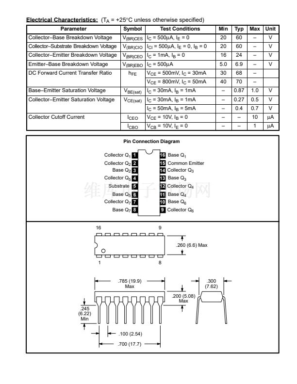
The NTE916 is a high current transistor array in a 16鈥揕ead DIP type package consisting of seven
silicon NPN transistors on a common monolithic substrate connected in a common鈥揺mitter config-
uration designed for directly driving seven鈥搒egment displays and light鈥揺mitting diodes (LED) dis-
plays. This device is also well suited for a variety of other drive applications including relay control
and thyristor firing.
Features:
D
Seven Transistors Permit a Wide Range of Applications
D
High Collector Current: I
C
= 100mA Max
D
Low Collector鈥揈mitter Saturation Voltage: V
CE(sat)
= 400mV Typ @ 50mA
Absolute Maximum Ratings:
(T
A
= +25擄C unless otherwise specified)
Power Dissipation (Total Package), P
D
. . . . . . . . . . . . . . . . . . . . . . . . . . . . . . . . . . . . . . . . . . . . 750mW
Per Transistor . . . . . . . . . . . . . . . . . . . . . . . . . . . . . . . . . . . . . . . . . . . . . . . . . . . . . . . . . . . . 500mW
Derate Linearly Above 55擄C . . . . . . . . . . . . . . . . . . . . . . . . . . . . . . . . . . . . . . . . . 6.67mW/擄C
Operating Ambient Temperature Range, T
A
. . . . . . . . . . . . . . . . . . . . . . . . . . . . . . . . . . 鈥?5擄 to +125擄C
Storage Temperature Range, T
stg
. . . . . . . . . . . . . . . . . . . . . . . . . . . . . . . . . . . . . . . . . . 鈥?5擄 to +150擄C
Lead Temperature (During Soldering, 1/16鈥?from case, 10sec max), T
L
. . . . . . . . . . . . . . . . . +265擄C
The Following Ratings Apply for Each Transistor in the Device
Collector鈥揈mitter Voltage, V
CEO
. . . . . . . . . . . . . . . . . . . . . . . . . . . . . . . . . . . . . . . . . . . . . . . . . . . . . . 16V
Collector鈥揃ase Voltage, V
CBO
. . . . . . . . . . . . . . . . . . . . . . . . . . . . . . . . . . . . . . . . . . . . . . . . . . . . . . . 20V
Collector鈥揝ubstrate Voltage (Note 1), V
CIO
. . . . . . . . . . . . . . . . . . . . . . . . . . . . . . . . . . . . . . . . . . . . 20V
Emitter鈥揃ase Voltage, V
EBO
. . . . . . . . . . . . . . . . . . . . . . . . . . . . . . . . . . . . . . . . . . . . . . . . . . . . . . . . . . 5V
Collector Current, I
C
. . . . . . . . . . . . . . . . . . . . . . . . . . . . . . . . . . . . . . . . . . . . . . . . . . . . . . . . . . . . . 100mA
Base Current, I
B
. . . . . . . . . . . . . . . . . . . . . . . . . . . . . . . . . . . . . . . . . . . . . . . . . . . . . . . . . . . . . . . . . 20mA
Note 1. The collector of each transistor of the NTE916 is isolated from the substrate by an integral
diode. The substrate must be connected to a voltage which is more negative that any collec-
tor voltage in order to maintain isolation between transistors and provide normal transistor
action. To avoid undesired coupling between transistors, the substrate terminal (Pin5)
should be maintained at either DC or signal (AC) ground. A suitable bypass capacitor can
be used to establish a signal ground.


 1
1
 2
2
