NTE906
Integrated Circuit
Dual, High Frequency, Differential Amplifier
Description:
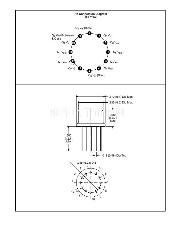
The NTE906 is an integrated circuit in a 12鈥揕ead TO5 type package consisting of two independent
differential amplifiers with associated constant鈥揷urrent transistors on a common monolithic sub-
strate. The six transistors which comprise the amplifiers are general鈥損urpose devices which exhibit
low 1/f noise and a value of f
T
in excess of 1GHz. These features make the NTE906 useful from DC
to 500MHz. Bias and load resistors have been omitted to provide maximum application flexibility.
The monolithic construction of the NTE906 provides close electrical and thermal matching of the am-
plifiers. This feature makes this device particularly useful in dual鈥揷hannel applications where
matched performance of the two channels is required.
Features:
D
Power Gain: 23dB (Typ) @ 200MHz
D
Noise Figure: 4.6dB (Typ) @ 200MHz
D
Two Different Amplifiers on a Common Substrate
D
Independently Accessible Input and Outputs
Absolute Maximum Ratings:
(T
A
= +25擄C unless otherwise specified)
Power Dissipation, P
D
Any One Transistor . . . . . . . . . . . . . . . . . . . . . . . . . . . . . . . . . . . . . . . . . . . . . . . . . . . . . . . 300mW
Total Package . . . . . . . . . . . . . . . . . . . . . . . . . . . . . . . . . . . . . . . . . . . . . . . . . . . . . . . . . . . 600mW
Derate Above +55擄C . . . . . . . . . . . . . . . . . . . . . . . . . . . . . . . . . . . . . . . . . . . . . . . . . . . 5mW/擄C
Operating Temperature Range, T
opr
. . . . . . . . . . . . . . . . . . . . . . . . . . . . . . . . . . . . . . . . 鈥?5擄 to +125擄C
Storage Temperature Range, T
stg
. . . . . . . . . . . . . . . . . . . . . . . . . . . . . . . . . . . . . . . . . . 鈥?5擄 to +150擄C
The following ratings apply for each transistor:
Collector鈥揈mitter Voltage, V
CEO
. . . . . . . . . . . . . . . . . . . . . . . . . . . . . . . . . . . . . . . . . . . . . . . . . . . . . . 15V
Collector鈥揃ase Voltage, V
CBO
. . . . . . . . . . . . . . . . . . . . . . . . . . . . . . . . . . . . . . . . . . . . . . . . . . . . . . . 20V
Collector鈥揝ubstrate Voltage (Note 1), V
CIO
. . . . . . . . . . . . . . . . . . . . . . . . . . . . . . . . . . . . . . . . . . . . 20V
Emitter鈥揃ase Voltage, V
EBO
. . . . . . . . . . . . . . . . . . . . . . . . . . . . . . . . . . . . . . . . . . . . . . . . . . . . . . . . . . 5V
Collector Current, I
C
. . . . . . . . . . . . . . . . . . . . . . . . . . . . . . . . . . . . . . . . . . . . . . . . . . . . . . . . . . . . . . 50mA
Note 1. The collector of each transistor is isolated from the substrate by an integral diode. The sub-
strate (Pin9) must be connected to the most negative point in the external circuit to maintain
isolation between transistors and to provide for normal transistor action.


 1
1
 2
2
 3
3
