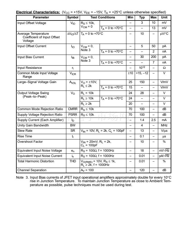
NTE858M
NTE858SM
Integrated Circuit
Dual, Low鈥揘oise JFET鈥揑nput Operational Amplifier
Description:
The NTE858M and NTE858SM are dual, low鈥搉oise JFET input operational amplifiers combining two
state鈥搊f鈥搕he鈥揳rt linear technologies on a single monolithic integrated circuit. Each internally com-
pensated operational amplifier has well matched high voltage JFET input devices for low input offset
voltage. The BIFET technology provides wide bandwidths and fast slew rates with low input bias cur-
rents, input offset currents, and supply currents. Moreover, these devices exhibit low鈥搉oise and low
harmonic distortion making them ideal for use in high鈥揻idelity audio amplifier applications.
Features:
D
Available in Two Different Package Types:
8鈥揕ead Mini DIP (NTE858M)
SOIC鈥? Surface Mount (NTE858SM)
D
Low Input Noise Voltage: 18nV鈭欻z Typ
D
Low Harmonic Distortion: 0.01% Typ
D
Low Input Bias and Offset Currents
D
High Input Impedance: 10
12
鈩?/div>
Typ
D
High Slew Rate: 13V/碌s Typ
D
Wide Gain Bandwidth: 4MHz Typ
D
Low Supply Current: 1.4mA per Amp
Absolute Maximum Ratings:
Supply Voltage
V
CC
. . . . . . . . . . . . . . . . . . . . . . . . . . . . . . . . . . . . . . . . . . . . . . . . . . . . . . . . . . . . . . . . . . . . . . . +18V
V
EE
. . . . . . . . . . . . . . . . . . . . . . . . . . . . . . . . . . . . . . . . . . . . . . . . . . . . . . . . . . . . . . . . . . . . . . . . 鈥?8V
Differential Input Voltage, V
ID
. . . . . . . . . . . . . . . . . . . . . . . . . . . . . . . . . . . . . . . . . . . . . . . . . . . . . . .
鹵30V
Input Voltage Range (Note 1), V
IDR
. . . . . . . . . . . . . . . . . . . . . . . . . . . . . . . . . . . . . . . . . . . . . . . . . .
鹵15V
Output Short鈥揅ircuit Duration (Note 2), t
S
. . . . . . . . . . . . . . . . . . . . . . . . . . . . . . . . . . . . . . Continuous
Power Dissipation, P
D
. . . . . . . . . . . . . . . . . . . . . . . . . . . . . . . . . . . . . . . . . . . . . . . . . . . . . . . . . . 680mW
Derate Above T
A
= +47擄C . . . . . . . . . . . . . . . . . . . . . . . . . . . . . . . . . . . . . . . . . . . . . . . . 10mW/擄C
Operating Ambient Temperature Range, T
A
. . . . . . . . . . . . . . . . . . . . . . . . . . . . . . . . . . . . . 0擄 to +70擄C
Storage Temperature Range, T
stg
. . . . . . . . . . . . . . . . . . . . . . . . . . . . . . . . . . . . . . . . . . 鈥?5擄 to +150擄C
Note 1. The magnitude of the input voltage must not exceed the magnitude of the supply voltage or
15V, whichever is less.
Note 2. The output may be shorted to GND or either supply. Temperature and/or supply voltages
must be limited to ensure that power dissipation ratungs are not exceeded.


 1
1
 2
2
 3
3
