NTE7074
Integrated Circuit
Module, 3 Output Positive Voltage
Regulator for VCR
Absolute Maximum Ratings:
(T
A
= +25擄C unless otherwise specified)
Maximum DC Input Voltage, V
IN
(DC) Max . . . . . . . . . . . . . . . . . . . . . . . . . . . . . . . . . . . . . . . . . . . . 30V
Maximum Average Output Current, I
O
Max
V
O
1 . . . . . . . . . . . . . . . . . . . . . . . . . . . . . . . . . . . . . . . . . . . . . . . . . . . . . . . . . . . . . . . . . . . . . . . 1.0A
V
O
2 . . . . . . . . . . . . . . . . . . . . . . . . . . . . . . . . . . . . . . . . . . . . . . . . . . . . . . . . . . . . . . . . . . . . . . . 1.0A
V
O
3 . . . . . . . . . . . . . . . . . . . . . . . . . . . . . . . . . . . . . . . . . . . . . . . . . . . . . . . . . . . . . . . . . . . . . . . 1.0A
Maximum Peak Output Current (Note 1), I
O
Max
V
O
1 . . . . . . . . . . . . . . . . . . . . . . . . . . . . . . . . . . . . . . . . . . . . . . . . . . . . . . . . . . . . . . . . . . . . . . . 2.0A
V
O
2 . . . . . . . . . . . . . . . . . . . . . . . . . . . . . . . . . . . . . . . . . . . . . . . . . . . . . . . . . . . . . . . . . . . . . . . 2.0A
V
O
3 . . . . . . . . . . . . . . . . . . . . . . . . . . . . . . . . . . . . . . . . . . . . . . . . . . . . . . . . . . . . . . . . . . . . . . . 2.0A
Operating Case Temperature, T
C
Max . . . . . . . . . . . . . . . . . . . . . . . . . . . . . . . . . . . . . . . . . . . . . +105擄C
Junction Temperature, T
J
Max . . . . . . . . . . . . . . . . . . . . . . . . . . . . . . . . . . . . . . . . . . . . . . . . . . . . +150擄C
Storage Temperature Range, T
stg
. . . . . . . . . . . . . . . . . . . . . . . . . . . . . . . . . . . . . . . . . . 鈥?0擄 to +105擄C
Thermal Resistance, Junction鈥搕o鈥揅ase, R
thJC
. . . . . . . . . . . . . . . . . . . . . . . . . . . . . . . . . . . . . . . 7擄C/W
Note 1. Peak Current: For 0.2sec Max.
Electrical Characteristics:
(T
A
= +25擄C unless otherwise specified)
Parameter
Output Voltage Setting
Output Cutoff Residual Voltage
Ripple Voltage
Temperature Coefficient
Input Regulation
Load Regulation
Minimum Input鈥揙utput Voltage Difference
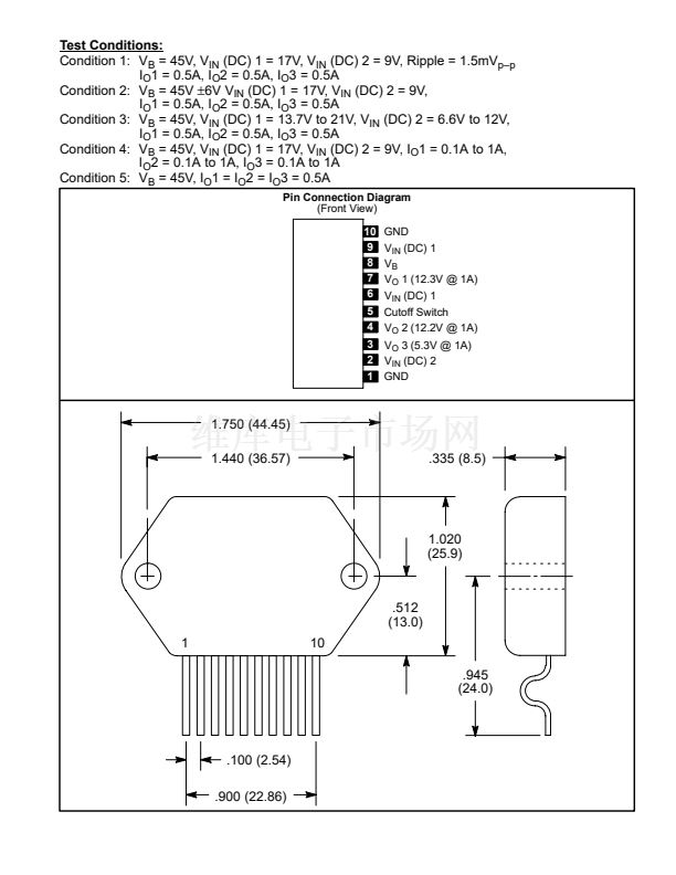
Test Conditions
Condition 1, Note 2
Condition 1
Condition 1
Condition 1
Condition 2
Condition 3
Condition 4
Condition 5
V
O
1
12.3鹵0.2
12.3鹵0.2
10
0.02
10
2
50
1.2
V
O
2
12.2鹵0.2
0.1
5
0.02
10
2
45
1.2
V
O3
5.3鹵0.8
0.1
5
0.02
2
2
45
1.2
mV/A Max
V Max
Unit
V
V Max
mV
p鈥損
Max
%/擄C Max
mV/V Max
Note 2. Measurement must be made within 1 to 2 sec. after input switch is ON.


 1
1
 2
2
