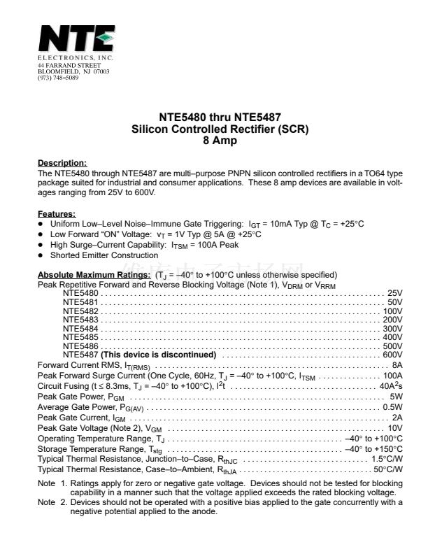
NTE5480 thru NTE5487
Silicon Controlled Rectifier (SCR)
8 Amp
Description:
The NTE5480 through NTE5487 are multi鈥損urpose PNPN silicon controlled rectifiers in a TO64 type
package suited for industrial and consumer applications. These 8 amp devices are available in volt-
ages ranging from 25V to 600V.
Features:
D
Uniform Low鈥揕evel Noise鈥揑mmune Gate Triggering: I
GT
= 10mA Typ @ T
C
= +25擄C
D
Low Forward 鈥淥N鈥?Voltage: v
T
= 1V Typ @ 5A @ +25擄C
D
High Surge鈥揅urrent Capability: I
TSM
= 100A Peak
D
Shorted Emitter Construction
Absolute Maximum Ratings:
(T
J
= 鈥?0擄 to +100擄C unless otherwise specified)
Peak Repetitive Forward and Reverse Blocking Voltage (Note 1), V
DRM
or V
RRM
NTE5480 . . . . . . . . . . . . . . . . . . . . . . . . . . . . . . . . . . . . . . . . . . . . . . . . . . . . . . . . . . . . . . . . . . . . 25V
NTE5481 . . . . . . . . . . . . . . . . . . . . . . . . . . . . . . . . . . . . . . . . . . . . . . . . . . . . . . . . . . . . . . . . . . . . 50V
NTE5482 . . . . . . . . . . . . . . . . . . . . . . . . . . . . . . . . . . . . . . . . . . . . . . . . . . . . . . . . . . . . . . . . . . . 100V
NTE5483 . . . . . . . . . . . . . . . . . . . . . . . . . . . . . . . . . . . . . . . . . . . . . . . . . . . . . . . . . . . . . . . . . . . 200V
NTE5484 . . . . . . . . . . . . . . . . . . . . . . . . . . . . . . . . . . . . . . . . . . . . . . . . . . . . . . . . . . . . . . . . . . . 300V
NTE5485 . . . . . . . . . . . . . . . . . . . . . . . . . . . . . . . . . . . . . . . . . . . . . . . . . . . . . . . . . . . . . . . . . . . 400V
NTE5486 . . . . . . . . . . . . . . . . . . . . . . . . . . . . . . . . . . . . . . . . . . . . . . . . . . . . . . . . . . . . . . . . . . . 500V
NTE5487
(This device is discontinued)
. . . . . . . . . . . . . . . . . . . . . . . . . . . . . . . . . . . . . . 600V
Forward Current RMS, I
T(RMS)
. . . . . . . . . . . . . . . . . . . . . . . . . . . . . . . . . . . . . . . . . . . . . . . . . . . . . . . . 8A
Peak Forward Surge Current (One Cycle, 60Hz, T
J
= 鈥?0擄 to +100擄C, I
TSM
. . . . . . . . . . . . . . . 100A
Circuit Fusing (t
鈮?/div>
8.3ms, T
J
= 鈥?0擄 to +100擄C), I
2
t . . . . . . . . . . . . . . . . . . . . . . . . . . . . . . . . . . . 40A
2
s
Peak Gate Power, P
GM
. . . . . . . . . . . . . . . . . . . . . . . . . . . . . . . . . . . . . . . . . . . . . . . . . . . . . . . . . . . . . 5W
Average Gate Power, P
G(AV)
. . . . . . . . . . . . . . . . . . . . . . . . . . . . . . . . . . . . . . . . . . . . . . . . . . . . . . . . 0.5W
Peak Gate Current, I
GM
. . . . . . . . . . . . . . . . . . . . . . . . . . . . . . . . . . . . . . . . . . . . . . . . . . . . . . . . . . . . . . 2A
Peak Gate Voltage (Note 2), V
GM
. . . . . . . . . . . . . . . . . . . . . . . . . . . . . . . . . . . . . . . . . . . . . . . . . . . . 10V
Operating Temperature Range, T
J
. . . . . . . . . . . . . . . . . . . . . . . . . . . . . . . . . . . . . . . . . . 鈥?0擄 to +100擄C
Storage Temperature Range, T
stg
. . . . . . . . . . . . . . . . . . . . . . . . . . . . . . . . . . . . . . . . . . 鈥?0擄 to +150擄C
Typical Thermal Resistance, Junction鈥搕o鈥揅ase, R
thJC
. . . . . . . . . . . . . . . . . . . . . . . . . . . . . . 1.5擄C/W
Typical Thermal Resistance, Case鈥搕o鈥揂mbient, R
thJA
. . . . . . . . . . . . . . . . . . . . . . . . . . . . . . . . 50擄C/W
Note 1. Ratings apply for zero or negative gate voltage. Devices should not be tested for blocking
capability in a manner such that the voltage applied exceeds the rated blocking voltage.
Note 2. Devices should not be operated with a positive bias applied to the gate concurrently with a
negative potential applied to the anode.


 1
1
 2
2
