NTE2968
MOSFET
N鈥揅hannel, Enhancement Mode
High Speed Switch
Features:
D
Avalanche Rugged Technology
D
Rugged Gate Oxide Technology
D
Low Input Capacitance
D
Improved Gate Charge
D
Extended Safe Operating Area
D
Lower Leakage Current
D
Low Static Drain鈥揝ource On鈥揝tate Resistance
Absolute Maximum Ratings:
Drain鈥揝ource Voltage, V
DSS
. . . . . . . . . . . . . . . . . . . . . . . . . . . . . . . . . . . . . . . . . . . . . . . . . . . . . . . . 200V
Drain Current, I
D
Continuous
T
C
= +25擄C . . . . . . . . . . . . . . . . . . . . . . . . . . . . . . . . . . . . . . . . . . . . . . . . . . . . . . . . . . . . . . . 45A
T
C
= +100擄C . . . . . . . . . . . . . . . . . . . . . . . . . . . . . . . . . . . . . . . . . . . . . . . . . . . . . . . . . . . . 27.8A
Pulsed (Note 1) . . . . . . . . . . . . . . . . . . . . . . . . . . . . . . . . . . . . . . . . . . . . . . . . . . . . . . . . . . . . . 180A
Gate鈥揝ource Voltage, V
GS
. . . . . . . . . . . . . . . . . . . . . . . . . . . . . . . . . . . . . . . . . . . . . . . . . . . . . . . . .
鹵30V
Gate Current (Pulsed), I
GM
. . . . . . . . . . . . . . . . . . . . . . . . . . . . . . . . . . . . . . . . . . . . . . . . . . . . . . . .
鹵1.5A
Single Pulsed Avalanche Energy (Note 2), E
AS
. . . . . . . . . . . . . . . . . . . . . . . . . . . . . . . . . . . . . . 675mJ
Avalanche Current (Note 1), I
AS
. . . . . . . . . . . . . . . . . . . . . . . . . . . . . . . . . . . . . . . . . . . . . . . . . . . . . . 45A
Repetitive Avalanche Energy (Note 1), E
AR
. . . . . . . . . . . . . . . . . . . . . . . . . . . . . . . . . . . . . . . . . 27.8mJ
Peak Diode Recovery dv/dt (Note 3), dv/dt . . . . . . . . . . . . . . . . . . . . . . . . . . . . . . . . . . . . . . . . . 5.0V/ns
Total Power Dissipation (T
C
= +25擄C), P
D
. . . . . . . . . . . . . . . . . . . . . . . . . . . . . . . . . . . . . . . . . . . 278W
Derate Above 25擄C . . . . . . . . . . . . . . . . . . . . . . . . . . . . . . . . . . . . . . . . . . . . . . . . . . . . . . 2.22W/擄C
Operating Junction Temperature Range, T
J
. . . . . . . . . . . . . . . . . . . . . . . . . . . . . . . . . . 鈥?5擄 to +150擄C
Storage Temperature Range, T
stg
. . . . . . . . . . . . . . . . . . . . . . . . . . . . . . . . . . . . . . . . . . 鈥?5擄 to +150擄C
Maximum Lead Temperature (During Soldering, 1/8鈥?from case, 5sec), T
L
. . . . . . . . . . . . . . +300擄C
Thermal Resistance:
Maximum Junction鈥搕o鈥揅ase, R
thJC
. . . . . . . . . . . . . . . . . . . . . . . . . . . . . . . . . . . . . . . . 0.45擄C/W
Typical Case鈥搕o鈥揝ink, R
thCS
. . . . . . . . . . . . . . . . . . . . . . . . . . . . . . . . . . . . . . . . . . . . . . 0.24擄C/W
Maximum Junction鈥搕o鈥揂mbient, R
thJA
. . . . . . . . . . . . . . . . . . . . . . . . . . . . . . . . . . . . . . . 40擄C/W
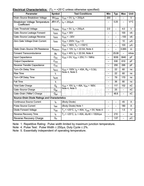
Note 1. Repetitive Rating: Pulse width limited by maximum junction temperature.
Note 2. L = 0.5mH, I
AS
= 45A, V
DD
= 25V, R
G
= 25鈩? Starting T
J
= +25擄C.
Note 3. I
SD
鈮?/div>
45A, di/dt
鈮?/div>
370A/碌s, V
DD
鈮?/div>
BV
DSS
, Starting T
J
= +25擄C.


 1
1
 2
2
 3
3
