The NTE2532 is a 32,768鈥揵it, ultraviolet鈥搇ight鈥揺rasable, electrically鈥損rogrammable read鈥搊nly
memory in a 24鈥揕ead DIP type package. This device is fabricated using N鈥揷hannel silicon鈥揼ate
technology for high speed and simple interface with MOS and bipolar circuits. All inputs (including
program data inputs) can be directly driven by Series 74 TTL circuits without the use of external pull鈥?/div>
up reistors, and each output can drive one Series 74 circuit without external resistors. The data out-
puts are three鈥搒tate for connecting mutiple devices to a common bus.
Since the NTE2532 operates from a single +5V supply (in the read mode), it is ideal for use in micro-
processor systems. One other (+25V) supply is needed for programming but all programming signals
are TTL level, requiring a single 10ms pulse. For programming outside of the system, existing
EPROM programmers can be used. Locations may be programmed singly, in blocks, or at random.
Total programming time for all bits is 41 seconds.
Features:
D
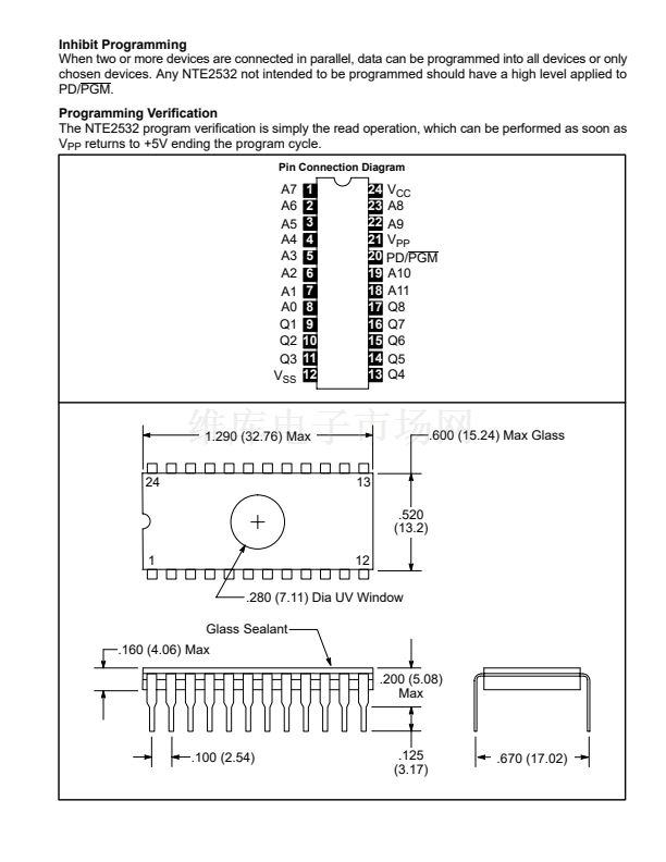
Organization: 4096 x 8
D
Single +5V Power Supply
D
All Inputs/Outputs Fully TTL Compatible
D
Static Operation (No Clocks, No Refresh)
D
Max Acces/Min Cycle Time: 300ns
D
8鈥揃it Output for Use in Microprocessor Based Systems
D
N鈥揅hannel Silicon鈥揋ate Technology
D
3鈥揝tate Output Buffers
D
Low Power Dissipation:
Active 鈥?400mW Typical
Standby 鈥?100mW Standby
D
Guaranteed DC Noise Immunity with Standard TTL Loads
D
No Pull鈥揢p Resistors Required
Absolute Maximum Ratings:
(T
A
= 0擄 to +70擄C, Note 1 unless otherwise specified)
Supply Voltage (Note 2), V
CC
. . . . . . . . . . . . . . . . . . . . . . . . . . . . . . . . . . . . . . . . . . . . . . . . 鈥?.3V to +7V
Supply Voltage (Note 2), V
PP
. . . . . . . . . . . . . . . . . . . . . . . . . . . . . . . . . . . . . . . . . . . . . . . 鈥?.3V to +28V
All Input Voltages (Note 1) . . . . . . . . . . . . . . . . . . . . . . . . . . . . . . . . . . . . . . . . . . . . . . . . . . . 鈥?.3V to +7V
Output Voltage (Operating, with Respect to V
SS
) . . . . . . . . . . . . . . . . . . . . . . . . . . . . . . . . 鈥?.3V to 7V
Operating Ambient Temperature Range, T
A
. . . . . . . . . . . . . . . . . . . . . . . . . . . . . . . . . . . . . 0擄 to +70擄C
Storage Temperature Range, T
stg
. . . . . . . . . . . . . . . . . . . . . . . . . . . . . . . . . . . . . . . . . . 鈥?5擄 to +150擄C
Note 1. Stresses beyond those listed under 鈥淎bsolute Maximum Ratings鈥?may cause permanent dam-
age to the device. This is a stress rating only and functional operation of the device at these
or any other conditions beyond those indicated in the 鈥淩ecommended Operation Conditions鈥?/div>
section of this specification is not implied. Exposure to absolute鈥搈aximum鈥搑ated conditions
for extended periods may affect device reliability.
Note 2. Under absolute maximum ratings, voltage values are with respect to the most negative supply
voltage, V
S
(substrate).


 1
1
 2
2
 3
3
 4
4
