NTE2319
Silicon NPN Transistor
High Voltage, High Speed Power Switch
Description:
The NTE2319 is a silicon NPN transistor in a TO3 type package designed for high voltage, high speed,
power switching in inductive circuits where fall time is critical. It is particularly suited for line鈥搊perated
switchmode applications.
Features:
D
Fast Turn鈥揙n Times @ T
C
= +100擄C:
Inductive Fall Time: 50ns Typ
Inductive Crossover Time: 90ns Typ
Inductive Storage Time: 800ns Typ
D
100擄C Performance Specified for:
Reverse鈥揃iased SOA with Inductive Loads
Switching Times with Inductive Loads
Saturation Voltages
Leakage Current
Applications:
D
Switching Regulators
D
Inverters
D
Solenoids
D
Relay Drivers
D
Motor Controls
D
Deflection Circuits
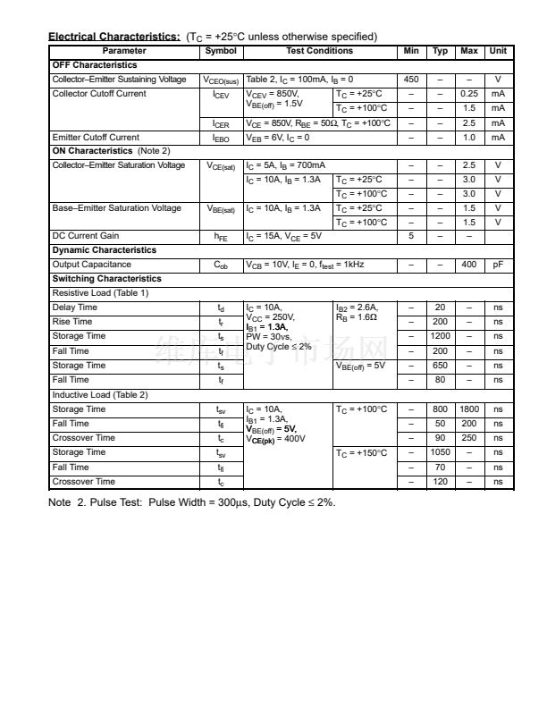
Absolute Maximum Ratings:
Collector鈥揈mitter Voltage, V
CEO
. . . . . . . . . . . . . . . . . . . . . . . . . . . . . . . . . . . . . . . . . . . . . . . . . . . . . 450V
Collector鈥揈mitter Voltage, V
CEV
. . . . . . . . . . . . . . . . . . . . . . . . . . . . . . . . . . . . . . . . . . . . . . . . . . . . . 850V
Emitter鈥揃ase Voltage, V
EB
. . . . . . . . . . . . . . . . . . . . . . . . . . . . . . . . . . . . . . . . . . . . . . . . . . . . . . . . . . . 6V
Collector Current, I
C
Continuous . . . . . . . . . . . . . . . . . . . . . . . . . . . . . . . . . . . . . . . . . . . . . . . . . . . . . . . . . . . . . . . . . . 15A
Peak (Note 1) . . . . . . . . . . . . . . . . . . . . . . . . . . . . . . . . . . . . . . . . . . . . . . . . . . . . . . . . . . . . . . . . 20A
Base Current, I
B
Continuous . . . . . . . . . . . . . . . . . . . . . . . . . . . . . . . . . . . . . . . . . . . . . . . . . . . . . . . . . . . . . . . . . . 10A
Peak (Note 1) . . . . . . . . . . . . . . . . . . . . . . . . . . . . . . . . . . . . . . . . . . . . . . . . . . . . . . . . . . . . . . . . 15A
Total Device Dissipation, P
D
T
C
= +25擄C . . . . . . . . . . . . . . . . . . . . . . . . . . . . . . . . . . . . . . . . . . . . . . . . . . . . . . . . . . . . . . . . 175W
T
C
= +100擄C . . . . . . . . . . . . . . . . . . . . . . . . . . . . . . . . . . . . . . . . . . . . . . . . . . . . . . . . . . . . . . . 100W
Derate Above 25擄C . . . . . . . . . . . . . . . . . . . . . . . . . . . . . . . . . . . . . . . . . . . . . . . . . . . . . . . . . 1W/擄C
Operating Junction Temperature Range, T
J
. . . . . . . . . . . . . . . . . . . . . . . . . . . . . . . . . . 鈥?5擄 to +200擄C
Storage Temperature Range, T
stg
. . . . . . . . . . . . . . . . . . . . . . . . . . . . . . . . . . . . . . . . . . 鈥?5擄 to +200擄C
Thermal Resistance, Junction鈥搕o鈥揅ase, R
thJC
. . . . . . . . . . . . . . . . . . . . . . . . . . . . . . . . . . . . . . . 1擄C/W
Lead Temperature (During Soldering, 1/8鈥?from case, 5sec), T
L
. . . . . . . . . . . . . . . . . . . . . . . +275擄C
Note 1. Pulse Test: Pulse Width
鈮?/div>
5碌s, Duty Cycle
next


 1
1
 2
2
 3
3
