The NTE2312 is a silicon NPN transistor in a TO220 type package designed for high鈥搗oltage, high鈥?/div>
speed power switching inductive circuits where fall time is critical. This device is particularly suited
for 115V and 220V switch鈥搈ode applications such as switching regulators, inverters, motor controls,
solenoid/relay drivers, and deflection circuits.
Absolute Maximum Ratings:
Collector鈥揈mitter Voltage, V
CEO(sus)
. . . . . . . . . . . . . . . . . . . . . . . . . . . . . . . . . . . . . . . . . . . . . . . . . 400V
Collector鈥揈mitter Voltage, V
CEV
. . . . . . . . . . . . . . . . . . . . . . . . . . . . . . . . . . . . . . . . . . . . . . . . . . . . . 700V
Emitter鈥揃ase Voltage, V
EBO
. . . . . . . . . . . . . . . . . . . . . . . . . . . . . . . . . . . . . . . . . . . . . . . . . . . . . . . . . . 9V
Collector Current, I
C
Continuous . . . . . . . . . . . . . . . . . . . . . . . . . . . . . . . . . . . . . . . . . . . . . . . . . . . . . . . . . . . . . . . . . . . 8A
Peak (Note 1) . . . . . . . . . . . . . . . . . . . . . . . . . . . . . . . . . . . . . . . . . . . . . . . . . . . . . . . . . . . . . . . . 16A
Base Current, I
B
Continuous . . . . . . . . . . . . . . . . . . . . . . . . . . . . . . . . . . . . . . . . . . . . . . . . . . . . . . . . . . . . . . . . . . . 4A
Peak (Note 1) . . . . . . . . . . . . . . . . . . . . . . . . . . . . . . . . . . . . . . . . . . . . . . . . . . . . . . . . . . . . . . . . . 8A
Emitter Current, I
E
Continuous . . . . . . . . . . . . . . . . . . . . . . . . . . . . . . . . . . . . . . . . . . . . . . . . . . . . . . . . . . . . . . . . . . 12A
Peak (Note 1) . . . . . . . . . . . . . . . . . . . . . . . . . . . . . . . . . . . . . . . . . . . . . . . . . . . . . . . . . . . . . . . . 24A
Total Power Dissipation (T
A
= +25擄C), P
D
. . . . . . . . . . . . . . . . . . . . . . . . . . . . . . . . . . . . . . . . . . . . . . 2W
Derate Above 25擄C . . . . . . . . . . . . . . . . . . . . . . . . . . . . . . . . . . . . . . . . . . . . . . . . . . . . . . 16mW/擄C
Total Power Dissipation (T
C
= +25擄C), P
D
. . . . . . . . . . . . . . . . . . . . . . . . . . . . . . . . . . . . . . . . . . . . 80W
Derate Above 25擄C . . . . . . . . . . . . . . . . . . . . . . . . . . . . . . . . . . . . . . . . . . . . . . . . . . . . . 640mW/擄C
Operating Junction Temperature Range, T
J
. . . . . . . . . . . . . . . . . . . . . . . . . . . . . . . . . . 鈥?5擄 to +150擄C
Storage Temperature Range, T
stg
. . . . . . . . . . . . . . . . . . . . . . . . . . . . . . . . . . . . . . . . . . 鈥?5擄 to +150擄C
Thermal Resistance, Junction鈥搕o鈥揅ase, R
thJC
. . . . . . . . . . . . . . . . . . . . . . . . . . . . . . . . . . . . 1.56擄C/W
Thermal Resistance, Junction鈥搕o鈥揂mbient, R
thJA
. . . . . . . . . . . . . . . . . . . . . . . . . . . . . . . . . . 62.5擄C/W
Lead Temperature (During Soldering, 1/8鈥?from case, 5sec), T
L
. . . . . . . . . . . . . . . . . . . . . . . +275擄C
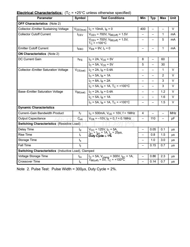
Note 1. Pulse Test: Pulse Width = 5ms, Duty Cycle
next


 1
1
 2
2
 3
3
