NTE2027
Integrated Circuit
Hex LED Digit Driver
Description:
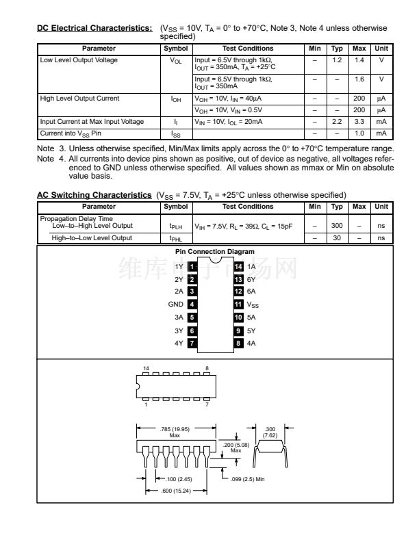
The NTE2027 is an interface circuit in a 14鈥揕ead DIP typ package designed to be used in conjunction
with MOS integrated circuits and common cathode LED鈥檚 in serially addressed multi鈥揹igit displays.
The number of drivers required for this time鈥搈ultiplexed system is minimized as a result of the seg-
ment鈥揳ddress鈥揳nd鈥揹igit鈥搒can method of LED drive.
Features:
D
Sink Capability Per Driver: 350mA
D
MOS Compatibility (Low Input Current)
D
Low Standby Power
D
High鈥揋ain Darlington Circuits
Absolute Maximum Ratings:
(Note 1)
Input Voltage Range (Note 2) . . . . . . . . . . . . . . . . . . . . . . . . . . . . . . . . . . . . . . . . . . . . . . . . . . 鈥?V to V
SS
Collector Output Voltage . . . . . . . . . . . . . . . . . . . . . . . . . . . . . . . . . . . . . . . . . . . . . . . . . . . . . . . . . . . . 10V
Collector Output to Input Voltage . . . . . . . . . . . . . . . . . . . . . . . . . . . . . . . . . . . . . . . . . . . . . . . . . . . . . 10V
Voltage at V
SS
Pin (with Respect to Any Other Device Pin) . . . . . . . . . . . . . . . . . . . . . . . . . . . . . . 10V
Collector Output Current
Each Collector Output . . . . . . . . . . . . . . . . . . . . . . . . . . . . . . . . . . . . . . . . . . . . . . . . . . . . . 350mA
All Collector Outputs . . . . . . . . . . . . . . . . . . . . . . . . . . . . . . . . . . . . . . . . . . . . . . . . . . . . . . . 600mA
Continuous Total Dissipation . . . . . . . . . . . . . . . . . . . . . . . . . . . . . . . . . . . . . . . . . . . . . . . . . . . . . . 800mW
Operating Temperature Range . . . . . . . . . . . . . . . . . . . . . . . . . . . . . . . . . . . . . . . . . . . . . . . . 0擄 to +70擄C
Storage Temperature Range . . . . . . . . . . . . . . . . . . . . . . . . . . . . . . . . . . . . . . . . . . . . . . . 鈥?5擄 to +150擄C
Lead Temperature (During Soldering, 10sec) . . . . . . . . . . . . . . . . . . . . . . . . . . . . . . . . . . . . . . . +300擄C
Note 1. 鈥淎bsolute Maximum Ratings鈥?are those values beyond which the safety of the device cannot
be guaranteed. Except for 鈥淥perating Temperature Range鈥?they are not meant to imply that
the device should be operated at these limits. The table of 鈥淓lectrical Characteristics鈥?pro-
vides conditions for actual device operation.
Note 2. The input is the only device pin which may be negative with respect to GND.


 1
1
 2
2
