NTE2024
Integrated Circuit
2鈥揇igit BCD鈥搕o鈥?鈥揝egment Decoder/Driver
Features:
D
Separate BCD inputs and segment outputs for each digit
D
Input loading less than 15碌A(chǔ)
D
I
2
L logic with buffered inputs and outputs
D
Internal input overrange protection circuit
D
5V supply operation
D
Internal biasing circuits
D
Output drive capability of 25mA per segment
D
Open collector outputs drive indicators directly
Description:
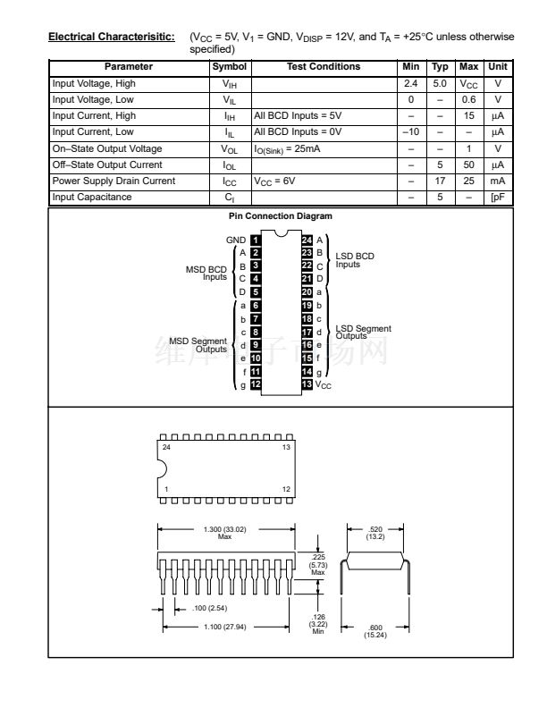
The NTE2024 is a monolithic integrated circuit intended for 2鈥揹igit display such as 鈥渘umbers鈥?for tV
and 鈥淐B鈥?channel selection, and other 0鈥?9 numerical or counting for consumer or industrial indicator
applications. It consists of two independent BCD鈥搕o鈥? segment decoder/drivers. Two sets of BCD
inputs are buffered with p鈥搉鈥損 differential amplifier stages internally referenced to 1.7V. Each of the
eight input terminals draws less than 15碌A(chǔ) and is provided with an internal protection circuit.
Decoding is accomplished with I
2
L ROM鈥檚. The fourteen output terminals are buffered with Darlington
pairs driving common鈥揺mitter output transistors. Each output is capable of sinking 25mA for an LED
common鈥揳node display device. The supply鈥搗oltage range (V
CC
) is intended to be 4.5V to 6V. The
output voltage (V
O
) must not exceed 12V, which provides for a wide range of common鈥揳node voltage
sources.
Absolute Maximum Ratings:
Supply Voltage, V
CC
. . . . . . . . . . . . . . . . . . . . . . . . . . . . . . . . . . . . . . . . . . . . . . . . . . . . . . . . . . . . . . . . 6V
Input鈥揤oltage (Min/Max) . . . . . . . . . . . . . . . . . . . . . . . . . . . . . . . . . . . . . . . . . . . . . . . . . . . . . . 鈥?.3V
CC
V
Input Current (Protection Circuit) . . . . . . . . . . . . . . . . . . . . . . . . . . . . . . . . . . . . . . . . . . . . . . . . . .
鹵10mA
Output Voltage, V
O
. . . . . . . . . . . . . . . . . . . . . . . . . . . . . . . . . . . . . . . . . . . . . . . . . . . . . . . . . . . . . . . . 12V
Output Segment Current, I
Display
. . . . . . . . . . . . . . . . . . . . . . . . . . . . . . . . . . . . . . . . . . . . . . . . . . . 25mA
Power Dissipation (T
A
鈮?/div>
+70擄C), P
D
. . . . . . . . . . . . . . . . . . . . . . . . . . . . . . . . . . . . . . . . . . . . . . . 400mW
Derate Linearly Above +70擄C . . . . . . . . . . . . . . . . . . . . . . . . . . . . . . . . . . . . . . . . . . . 8.7mW/擄C
Operating Ambient temperature Range, T
opr
. . . . . . . . . . . . . . . . . . . . . . . . . . . . . . . . . . . . 0擄 to 70擄C
StorageTemperature range, T
stg
. . . . . . . . . . . . . . . . . . . . . . . . . . . . . . . . . . . . . . . . . . . . 鈥?5擄 to +150擄C
Lead Temperature (During Soldering, 1/16鈥?/div>
鹵
1/32鈥?from case, 10sec max), T
L
. . . . . . . . . . +265擄C


 1
1
 2
2
