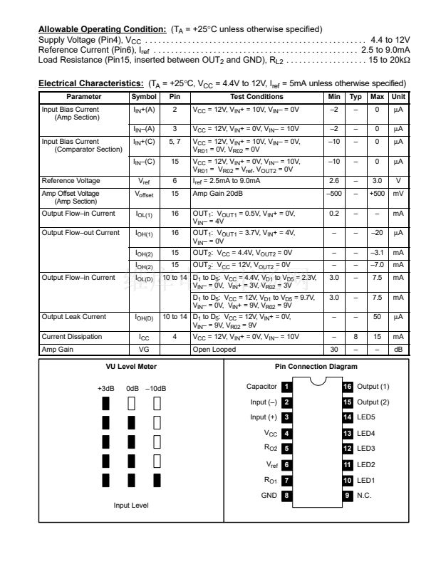
NTE1514 and NTE1515
Integrated Circuit
5鈥揝tep LED Driver for Logarithmic Scale
Features:
D
Useful for Both AC and DC Level Meter as VU Meter or Signal Meter
D
Wide Supply Voltage Ramge: V
CC
= 4.4V to 12V
D
DC Amplifier Included
Comparator Level:
(T
A
= +25擄C, V
CC
= 6V, I
ref
= 5mA)
NTE1514
Level
D5
D4
D3
D2
D1
Pin
14
13
12
11
10
Test Conditions
V
R02
= 2.6V to 3V, V
R02
= 0V
V
R02
= 2.6V to 3V, V
R02
= 0V
V
R02
= 2.6V to 3V, V
R02
= 0V
V
R02
= 2.6V to 3V, V
R02
= 0V
V
R02
= 2.6V to 3V, V
R02
= 0V
Min
5.5
2.5
鈥?.5
鈥?.0
鈥?2
Typ
6.0
3.0
0
鈥?.0
鈥?0
Max
6.5
3.5
0.5
鈥?.0
鈥?.0
Min
1.6
鈥?.4
鈥?.6
鈥?.0
鈥?7
NTE1515
Typ
2.0
0
鈥?.0
鈥?.0
鈥?5
Max
2.4
+0.4
鈥?.4
鈥?.0
鈥?3
Unit
dB
dB
dB
dB
dB
Note 1. Definition of 0dB:
when voltage of OUT
2
is 2.37V (R
02
= 3V, R
01
= 0V).
when voltage of OUT
2
is 1.50V (R
02
= 3V, R
01
= 0V).
Absolute Maximum Ratings:
(T
A
= +25擄C unless otherwise specified)
Maximum Supply Voltage (Pin4), V
CC
max . . . . . . . . . . . . . . . . . . . . . . . . . . . . . . . . . . . . 鈥?.3V to +14V
Input Voltage (Pin2, Pin3), V
IN
. . . . . . . . . . . . . . . . . . . . . . . . . . . . . . . . . . . . . . . . . . . . . . 鈥?.3V to +14V
Current at Pin C (Pin1), I
C
. . . . . . . . . . . . . . . . . . . . . . . . . . . . . . . . . . . . . . . . . . . . . . . . . . 0.1mA to 2mA
Output Voltage,
Pin16 (Note 2), V
OUT(1)
. . . . . . . . . . . . . . . . . . . . . . . . . . . . . . . . . . . . . . . . . . . . . . 鈥?.3V to +12V
Pin15, V
OUT(2)
. . . . . . . . . . . . . . . . . . . . . . . . . . . . . . . . . . . . . . . . . . . . . . . . . . . . . . 鈥?.3V to +12V
Pin10 to Pin14, V
OUT
. . . . . . . . . . . . . . . . . . . . . . . . . . . . . . . . . . . . . . . . . . . . . . . . . 鈥?.3V to 14V
Reference Current (Pin6), I
ref
. . . . . . . . . . . . . . . . . . . . . . . . . . . . . . . . . . . . . . . . . . . . . . . . . . 0 to 10mA
Allowable Power Dissipation (T
A
= +55擄C, Total), P
d
max . . . . . . . . . . . . . . . . . . . . . . . . . . . . . 500mW
Operating Temperature Range, T
opr
. . . . . . . . . . . . . . . . . . . . . . . . . . . . . . . . . . . . . . . . . 鈥?0擄 to +60擄C
Storage Temperature Range, T
stg
. . . . . . . . . . . . . . . . . . . . . . . . . . . . . . . . . . . . . . . . . . 鈥?0擄 to +125擄C
Note 2. When OUT
1
is off and OUT
2
is connected to GND (Pin8) through 12k鈩?
Note 3. Notice inhibit to supply any voltage to input and output pin larger than V
CC
+0.3V (Especially
beware of power switch on). Pin D
1
to D
5
should be connected to V
CC
at no use of LED鈥檚.


 1
1
 2
2
 3
3
