NLSF3T126
Quad Bus Buffer
with 3-State Control Inputs
The NLSF3T126 is a high speed CMOS quad bus buffer fabricated
with silicon gate CMOS technology. It achieves noninverting high
speed operation similar to equivalent Bipolar Schottky TTL while
maintaining CMOS low power dissipation.
The NLSF3T126 requires the 3-state control input (OE) to be set
Low to place the output into high impedance.
The T126 inputs are compatible with TTL levels. This device can be
used as a level converter for interfacing 3.3 V to 5.0 V, because it has
full 5.0 V CMOS level output swings.
The NLSF3T126 input structures provide protection when voltages
between 0 V and 5.5 V are applied, regardless of the supply voltage.
The output structures also provide protection when V
CC
= 0 V. These
input and output structures help prevent device destruction caused by
supply voltage - input/output voltage mismatch, battery backup, hot
insertion, etc.
The internal circuit is composed of three stages, including a buffer
output which provides high noise immunity and stable output. The
inputs tolerate voltages up to 7.0 V, allowing the interface of 5.0 V
systems to 3.0 V systems.
http://onsemi.com
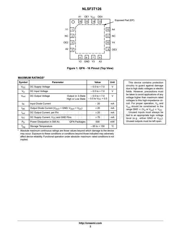
QFN-16
CASE 485G
MARKING
DIAGRAM
16
1
XXX
ALYW
鈥?/div>
鈥?/div>
鈥?/div>
鈥?/div>
鈥?/div>
鈥?/div>
鈥?/div>
鈥?/div>
鈥?/div>
鈥?/div>
鈥?/div>
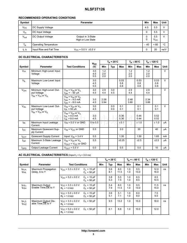
High Speed: t
PD
= 3.8 ns (Typ) at V
CC
= 5.0 V
Low Power Dissipation: I
CC
= 4.0
mA
(Max) at T
A
= 25擄C
TTL-Compatible Inputs: V
IL
= 0.8 V; V
IH
= 2.0 V
Power Down Protection Provided on Inputs
Balanced Propagation Delays
Designed for 2.0 V to 5.5 V Operating Range
Low Noise: V
OLP
= 0.8 V (Max)
Pin and Function Compatible with Other Standard Logic Families
Latchup Performance Exceeds 300 mA
ESD Performance: HBM > 2000 V; Machine Model > 200 V
Chip Complexity: 72 FETs or 18 Equivalent Gates
LOGIC DIAGRAM
Active-High Output Enables
A1
OE1
A2
OE2
A3
OE3
A4
OE4
16
15
4
3
8
9
12
13
10
Y4
7
Y3
5
Y2
1
Y1
(TOP VIEW)
A
WL
Y
WW
= Assembly Location
= Wafer Lot
= Year
= Work Week
ORDERING INFORMATION
Device
NLSF3T126MNR2
Package
QFN
Shipping
3000 Units/
Tape & Reel
FUNCTION TABLE
NLSF3T126
Inputs
A
H
L
X
OE
L
L
H
Output
Y
H
L
Z
漏
Semiconductor Components Industries, LLC, 2003
1
April, 2003 - Rev.0
Publication Order Number:
NLSF3T126/D
NLSF3T126/D相關(guān)型號PDF文件下載
-
型號
版本
描述
廠商
下載
-
英文版
Quad 2-Input NOR Gate
-
英文版
Quad 2-Input AND Gate
-
英文版
Serial (SPI) Tri-Color LED Driver
ONSEMI
-
英文版
Serial (SPI) Tri-Color LED Driver
ONSEMI [ON...
-
英文版
Hex D Flip-Flop with Common Clock And Reset
-
英文版
Keypad Multiplexer
ONSEMI [ON Semi...
-
英文版
Quad Bus Buffer
ONSEMI
-
英文版
Quad Bus Buffer
ONSEMI [ON...
-
英文版
Quad 2-Input NOR Gate
ETC
-
英文版
Quad 2-Input NOR Gate
-
英文版
Quad 2-Input AND Gate
ETC
-
英文版
Quad 2-Input AND Gate
-
英文版
Quad Bus Buffer
ONSEMI
-
英文版
Quad Bus Buffer
ONSEMI [ON...
-
英文版
Quad Bus Buffer
-
英文版
Serial (SPI) Tri-Color LED Driver
ETC
-
英文版
Serial (SPI) Tri-Color LED Driver
-
英文版
Hex D Flip-Flop with Common Clock And Reset
ETC
-
英文版
Hex D Flip-Flop with Common Clock And Reset
-
英文版
Quad 2−Input NOR Gate
ONSEMI [ON Semi...


 1
1
 2
2
 3
3
 4
4
 5
5
 6
6
 7
7
 8
8
