NL74VCXH16374
Low-Voltage 1.8/2.5/3.3V
16-Bit D-Type Flip-Flop
With 3.6V鈥揟olerant Inputs and Outputs
(3鈥揝tate, Non鈥揑nverting)
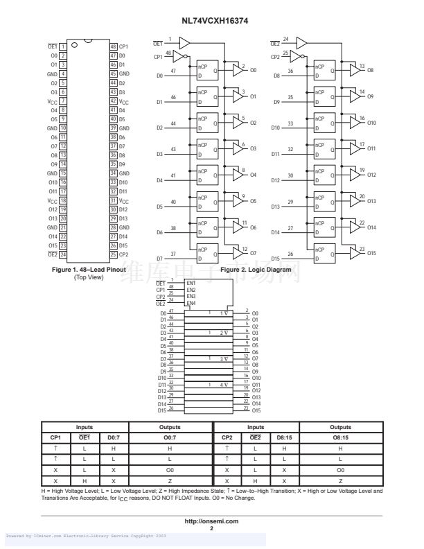
The NL74VCXH16374 is an advanced performance, non鈥搃nverting
16鈥揵it D鈥搕ype flip鈥揻lop. It is designed for very high鈥搒peed, very
low鈥損ower operation in 1.8V, 2.5V or 3.3V systems. The VCX16374
is byte controlled, with each byte functioning identically, but
independently. Each byte has separate Output Enable and Clock Pulse
inputs. These control pins can be tied together for full 16鈥揵it
operation.
When operating at 2.5V (or 1.8V) the part is designed to tolerate
voltages it may encounter on either inputs or outputs when interfacing
to 3.3V busses. It is guaranteed to be over鈥搗oltage tolerant to 3.6V.
The NL74VCXH16374 consists of 16 edge鈥搕riggered flip鈥揻lops
with individual D鈥搕ype inputs and 3.6V鈥搕olerant 3鈥搒tate outputs. The
clocks (CPn) and Output Enables (OEn) are common to all flip鈥揻lops
within the respective byte. The flip鈥揻lops will store the state of
individual D inputs that meet the setup and hold time requirements on
the LOW鈥搕o鈥揌IGH Clock (CP) transition. With the OE LOW, the
contents of the flip鈥揻lops are available at the outputs. When the OE is
HIGH, the outputs go to the high impedance state. The OE input level
does not affect the operation of the flip鈥揻lops. The data inputs include
active bushold circuitry, eliminating the need for external pull鈥搖p
resistors to hold unused or floating inputs at a valid logic state.
http://onsemi.com
48
1
TSSOP鈥?8
DT SUFFIX
CASE 1201
MARKING DIAGRAM
48
NL74VCXH16374DT
AWLYYWW
1
A
WL
YY
WW
= Assembly Location
= Wafer Lot
= Year
= Work Week
鈥?/div>
Designed for Low Voltage Operation: VCC = 1.65鈥?.6V
鈥?/div>
3.6V Tolerant Inputs and Outputs
鈥?/div>
High Speed Operation: 3.0ns max for 3.0 to 3.6V
鈥?/div>
鈥?/div>
鈥?/div>
鈥?/div>
鈥?/div>
鈥?/div>
鈥?/div>
3.9ns max for 2.3 to 2.7V
7.8ns max for 1.65 to 1.95V
Static Drive:
鹵24mA
Drive at 3.0V
鹵18mA
Drive at 2.3V
鹵6mA
Drive at 1.65V
Supports Live Insertion and Withdrawal
Includes Active Bushold to Hold Unused or Floating Inputs at a Valid
Logic State
IOFF Specification Guarantees High Impedance When VCC = 0V
鈥?/div>
Near Zero Static Supply Current in All Three Logic States (20碌A(chǔ))
Substantially Reduces System Power Requirements
Latchup Performance Exceeds
鹵300mA
@ 125擄C
ESD Performance: Human Body Model >2000V; Machine Model
>200V
Pins
OEn
CPn
D0鈥揇15
O0鈥揙15
PIN NAMES
Function
Output Enable Inputs
Clock Pulse Inputs
Inputs
Outputs
ORDERING INFORMATION
Device
NL74VCXH16374DT
NL74VCXH16374DTR
Package
TSSOP
TSSOP
Shipping
39 / Rail
2500 / Reel
鈥燦OTE: To ensure the outputs activate in the 3鈥搒tate condition, the output
enable pins should be connected to VCC through a pull鈥搖p resistor. The
value of the resistor is determined by the current sinking capability of the
output connected to the OE pin.
漏
Semiconductor Components Industries, LLC, 2000
1
May, 2000 鈥?Rev. 0
Powered by ICminer.com Electronic-Library Service CopyRight 2003
Publication Order Number:
NL74VCXH16374/D
NL74VCXH16374DTR相關(guān)型號(hào)PDF文件下載
-
型號(hào)
版本
描述
廠商
下載
-
英文版
THYRATRON TUBES 4 Amperes dc - 50 Amperes Peak
ETC [ETC]
-
英文版
THYRATRON TUBES 4 Amperes dc - 50 Amperes Peak
ETC [ETC]
-
英文版
Quad 4-Bit Buffer/Driver
ETC
-
英文版
Quad 4-Bit Buffer/Driver
ETC
-
英文版
Dual 8-bit Bus Transceiver
ETC
-
英文版
8-Bit D-Type Latch
ETC
-
英文版
16-Bit D-Type Flip-Flop
ETC
-
英文版
Quad 4-Bit Buffer/Driver
ETC
-
英文版
Quad 4-Bit Buffer/Driver
ETC
-
英文版
Dual 8-bit Bus Transceiver
ETC
-
英文版
8-Bit D-Type Latch
ETC
-
英文版
16-Bit D-Type Flip-Flop
ETC
-
英文版
Quad 4-Bit Buffer/Driver
ETC
-
英文版
Dual 8-bit Bus Transceiver
ETC
-
英文版
8-Bit D-Type Latch
ETC
-
英文版
16-Bit D-Type Flip-Flop
ETC
-
英文版
Quad 4-Bit Buffer/Driver
ETC
-
英文版
Dual 8-bit Bus Transceiver
ETC
-
英文版
8-Bit D-Type Latch
ETC
-
英文版
16-Bit D-Type Flip-Flop
ETC


 1
1
 2
2
 3
3
 4
4
 5
5
 6
6
 7
7
 8
8
 9
9
 10
10
 11
11
 12
12
