鈥?/div>
Extremely High Speed: t
PD
2.4 ns (typical) at V
CC
= 5 V
Designed for 1.65 V to 5.5 V V
CC
Operation
Over Voltage Tolerant Inputs
L
VTTL
Compatible 鈥?Interface Capability with 5 V TTL Logic with
V
CC
= 3 V
LVCMOS Compatible
24 mA Balanced Output Sink and Source Capability
Near Zero Static Supply Current Substantially Reduces System
Power Requirements
Replacement for NC7SZ86
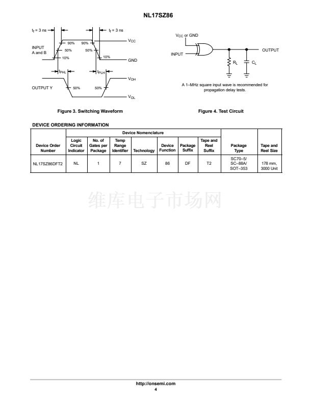
Figure 1.
http://onsemi.com
MARKING
DIAGRAM
5
1
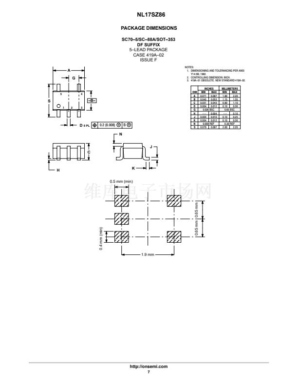
SC70鈥?/SC鈥?8A/SOT鈥?53
DF SUFFIX
CASE 419A
d = Date Code
L8
d
Pin 1
PIN ASSIGNMENT
1
2
IN B
1
5
V
CC
3
4
IN A
2
5
IN B
IN A
GND
OUT Y
V
CC
FUNCTION TABLE
GND
3
4
OUT Y
Inputs
A
B
L
H
L
H
Output
Y
L
H
H
L
Figure 1. Pinout
(Top View)
L
L
H
H
IN A
IN B
=1
OUT Y
Figure 2. Logic Symbol
ORDERING INFORMATION
See detailed ordering and shipping information in the package
dimensions section on page 4 of this data sheet.
漏
Semiconductor Components Industries, LLC, 2002
1
October, 2002 鈥?Rev. 2
Publication Order Number:
NL17SZ86/D


 1
1
 2
2
 3
3
 4
4
 5
5
 6
6
 7
7
 8
8
