鈥?/div>
Extremely High Speed: t
PD
2.6 ns (typical) at V
CC
= 5.0 V
Designed for 1.65 V to 5.5 V V
CC
Operation
Over Voltage Tolerant Inputs and Outputs
LVTTL Compatible 鈭?Interface Capability With 5.0 V TTL Logic
with V
CC
= 3.0 V
LVCMOS Compatible
24 mA Balanced Output Sink and Source Capability
Near Zero Static Supply Current Substantially Reduces System
Power Requirements
3鈭扴tate OE Input is Active HIGH
Replacement for NC7SZ126
Chip Complexity = 36 Feet
http://onsemi.com
MARKING
DIAGRAM
5
5
1
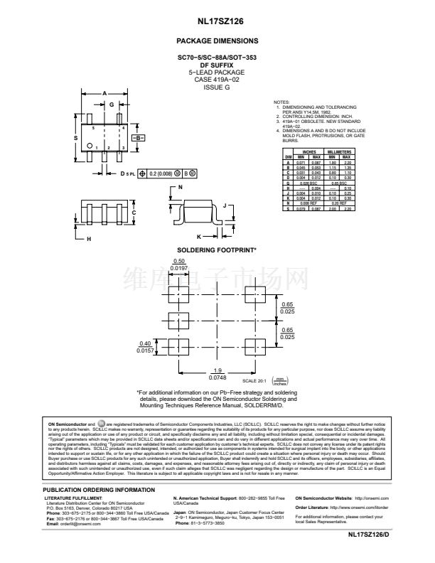
SC70鈭?/SC鈭?8A/SOT鈭?53
DF SUFFIX
CASE 419A
1
d = Date Code
M2
d
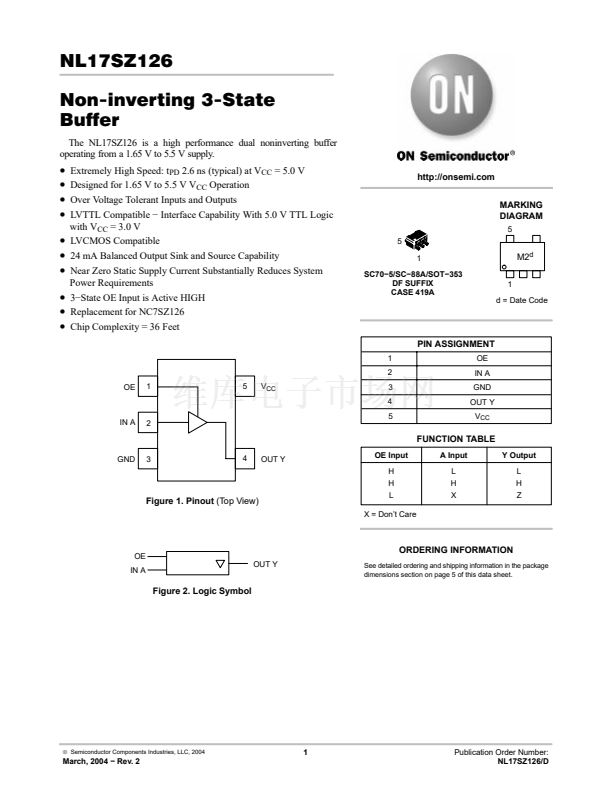
PIN ASSIGNMENT
1
2
OE
1
5
V
CC
3
4
IN A
2
5
OE
IN A
GND
OUT Y
V
CC
FUNCTION TABLE
GND
3
4
OUT Y
OE Input
H
H
L
X = Don鈥檛 Care
A Input
L
H
X
Y Output
L
H
Z
Figure 1. Pinout
(Top View)
OE
IN A
OUT Y
ORDERING INFORMATION
See detailed ordering and shipping information in the package
dimensions section on page 5 of this data sheet.
Figure 2. Logic Symbol
漏
Semiconductor Components Industries, LLC, 2004
1
March, 2004 鈭?Rev. 2
Publication Order Number:
NL17SZ126/D


 1
1
 2
2
 3
3
 4
4
 5
5
 6
6
