鈥?/div>
Chip Complexity: FETs = TBD
http://onsemi.com
MARKING
DIAGRAM
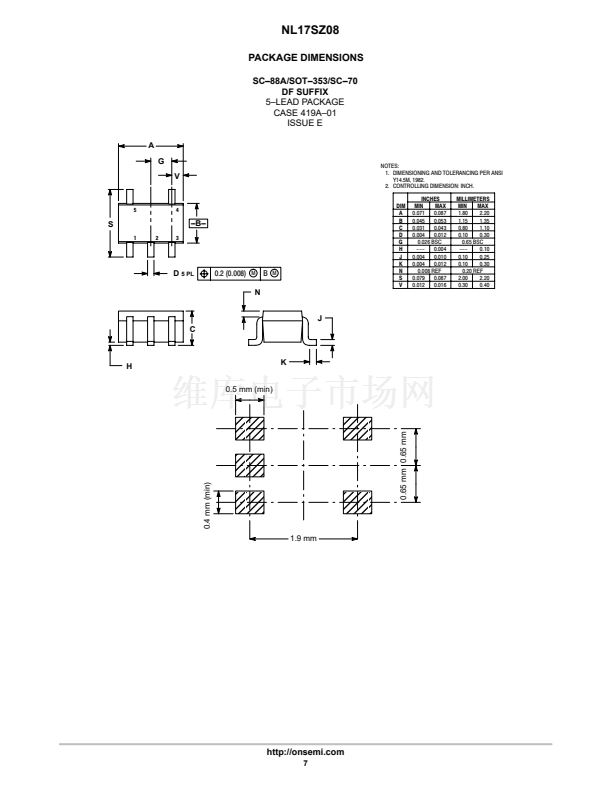
SC鈥?8A / SOT鈥?53/SC鈥?0
DF SUFFIX
CASE 419A
V1
d
Pin 1
d = Date Code
IN B
1
5
V
CC
TSOP鈥?/SOT鈥?3/SC鈥?9
DT SUFFIX
CASE 483
V1
d
IN A
2
Pin 1
d = Date Code
4
OUT Y
GND
3
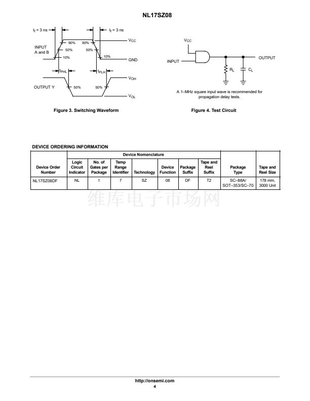
ORDERING INFORMATION
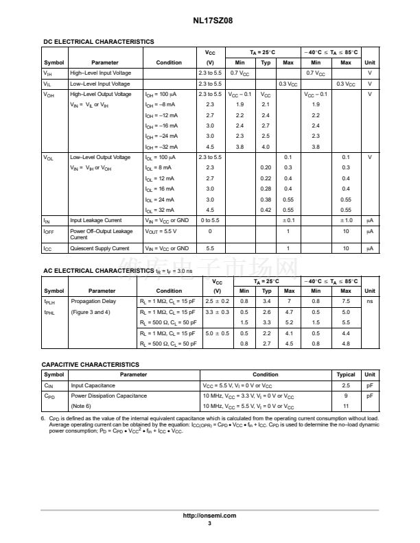
Figure 1. Pinout
(Top View)
See detailed ordering and shipping information in the package
dimensions section on page 4 of this data sheet.
IN A
IN B
&
OUT Y
Figure 2. Logic Symbol
PIN ASSIGNMENT
Pin
1
2
3
4
5
6
7
8
Function
A1
B1
Y2
GND
A2
B2
Y1
V
CC
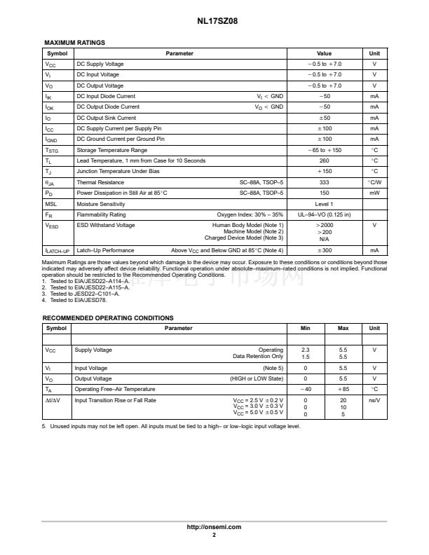
A
L
L
H
H
B
L
H
L
H
FUNCTION TABLE
Input
Output
Y=A+B
Y
H
L
L
L
This document contains information on a product under development. ON Semiconductor
reserves the right to change or discontinue this product without notice.
漏
Semiconductor Components Industries, LLC, 2001
1
May, 2001 鈥?Rev. 0
Publication Order Number:
NL17SZ08/D


 1
1
 2
2
 3
3
 4
4
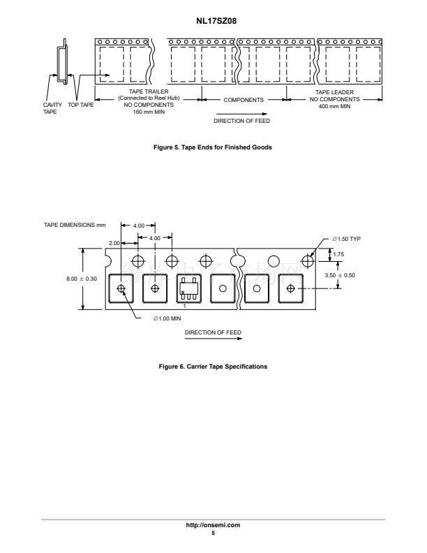 5
5
 6
6
 7
7
 8
8
