鈥?/div>
Tiny SOT- 353 and SOT- 553 Packages
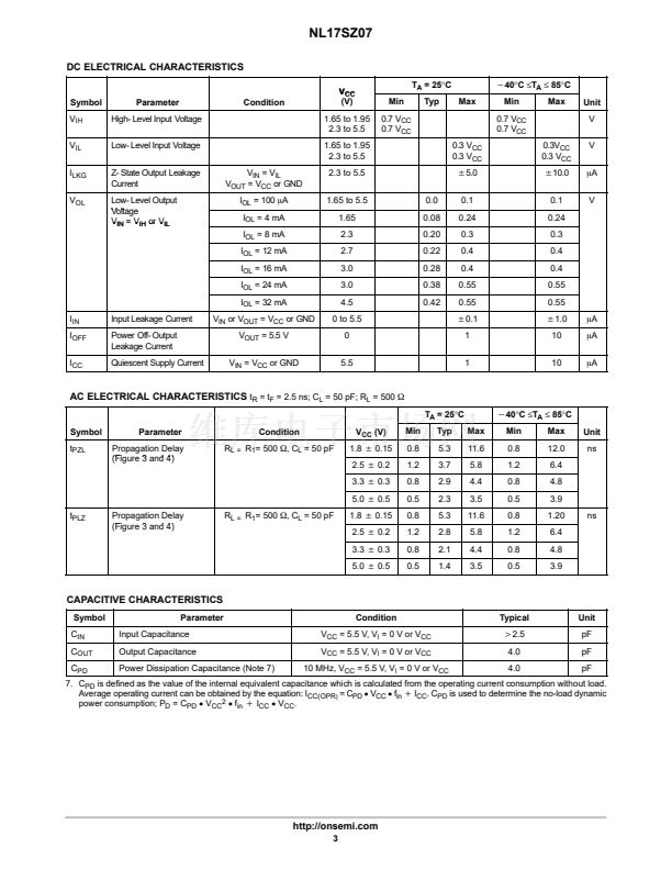
Extremely High Speed: t
PD
2.5 ns (typical) at V
CC
= 5 V
Designed for 1.65 V to 5.5 V V
CC
Operation, CMOS Compatible
Over Voltage Tolerant Inputs V
IN
may be Between 0 and 7.0 V for
V
CC
Between 0.5 and 5.4 V
TTL Compatible - Interface Capability with 5.0 V TTL Logic with
V
CC
= 2.7 V to 3.6 V
LVCMOS Compatible
24 mA Output Sink Capability, Pull-up may be between 0 and 7.0 V
Near Zero Static Supply Current Substantially Reduces System
Power Requirements
Chip Complexity: FET = 20
= Device Marking
= One Digit Date Code
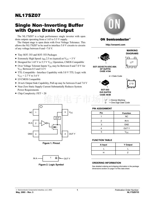
PIN ASSIGNMENT
NC
1
OVT
IN A
2
5
V
CC
Pin
1
2
3
4
5
GND
3
4
OUT Y
Function
NC
IN A
GND
OUT Y
V
CC
FUNCTION TABLE
Figure 1. Pinout
A Input
L
H
IN A
1
OUT Y
Y Output
L
Z
Figure 2. Logic Symbol
ORDERING INFORMATION
See detailed ordering and shipping information in the package
dimensions section on page 4 of this data sheet.
漏
Semiconductor Components Industries, LLC, 2003
1
May, 2003 - Rev. 3
Publication Order Number:
NL17SZ07/D


 1
1
 2
2
 3
3
 4
4
 5
5
 6
6
 7
7
 8
8
