NJG1112PB1
PDC Dual Band LNA GaAs MMIC
GENERAL DESCRIPTION
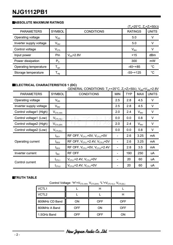
The NJG1112PB1 is a dual band low noise amplifier for
800MHz and 1500MHz band. The band switching between
800MHz CD, A Band and 1500MHz is made by 2 bit
control signal by using inverter circuit included in this IC.
The ultra small and thin FFP12-B1 is applied.
PACKAGE OUTLINE
NJG1112PB1
FEATURES
Low voltage operation
Low current consumption
Low control current
High gain
Low noise figure
High input IP3
Ultra small & thin package
+2.8V typ.
+2.6mA typ.@800MHz CD, A Band
+2.8mA typ.@1.5GHz Band
20uA typ.
18.5dB typ. @f=830MHz
18dB typ. @f=878MHz
17.5dB typ. @f=1490MHz
1.6dB typ. @f=830MHz
1.5dB typ. @f=878MHz
1.15dB typ. @f=1490MHz
-7dBm typ. @f=830.0+830.1MHz
-7dBm typ. @f=878.0+878.1MHz
-5dBm typ. @f=1490.0+1490.1MHz
FFP12-B1 (Package size: 2.0x2.0x0.85mm)
PIN CONFIGURATION
(Top View)
9
8
7
10
11
12
6
5
4
1
2
3
Pin Connection
1.GND
2.VCTL1
3.VCTL2
4.VINV
5.RFOUT1(800MHz Band)
6.GND
7.RFOUT2(1.5GHz Band)
8.GND
9.RFIN3(1.5GHz Band)
10.RFIN2(800MHz A Band)
11.GND
12.RFIN1(800MHz CD Band)
Note: The specifications and description listed in this catalog are subject to change without prior notice.
-1-


 1
1
 2
2
 3
3
 4
4
 5
5
 6
6
 7
7
 8
8
 9
9
 10
10
 11
11
 12
12
 13
13
 14
14
 15
15
 16
16
 17
17
