鈥?/div>
Emitter Ballasting for Short-Circuit Capability
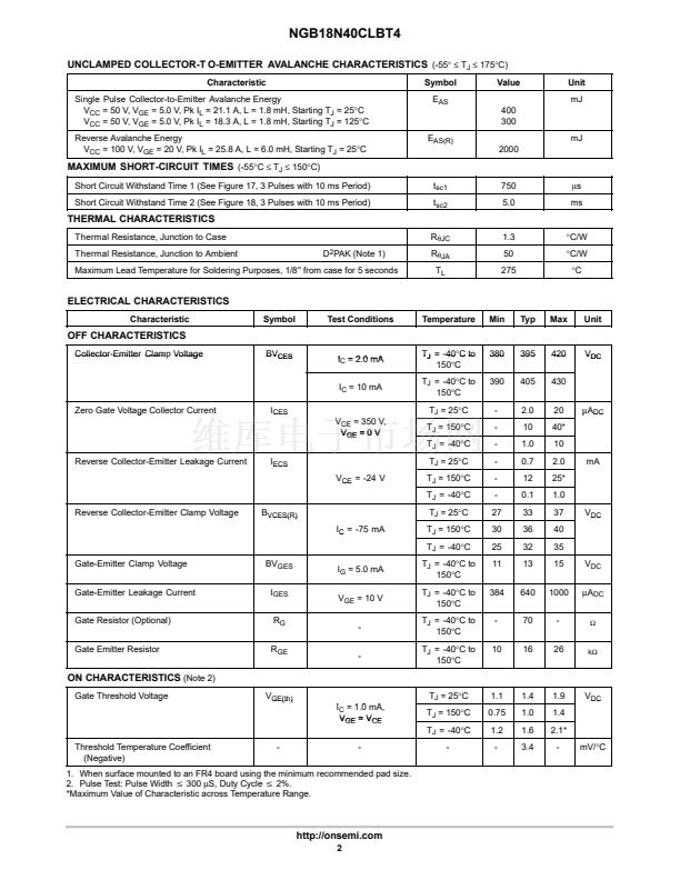
MAXIMUM RATINGS
(T
J
= 25擄C unless otherwise noted)
Rating
Collector-Emitter Voltage
Collector-Gate Voltage
Gate-Emitter Voltage
Collector Current-Continuous
@ T
C
= 25擄C - Pulsed
ESD (Human Body Model)
R = 1500
鈩?
C = 100 pF
ESD (Machine Model) R = 0
鈩?
C = 200 pF
Total Power Dissipation @ T
C
= 25擄C
Derate above 25擄C
Operating and Storage Temperature Range
Symbol
V
CES
V
CER
V
GE
I
C
ESD
8.0
ESD
P
D
T
J
, T
stg
800
115
0.77
-55 to
+175
V
Watts
W/擄C
擄C
1
Gate
2
Collector
3
Emitter
Value
430
430
18
18
50
Unit
V
DC
V
DC
V
DC
A
DC
A
AC
kV
1
http://onsemi.com
18 AMPS
400 VOLTS
V
CE(on)
3
2.0 V @
I
C
= 10 A, V
GE
.
4.5 V
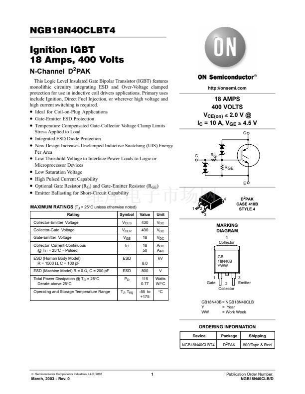
C
G
RG
RGE
E
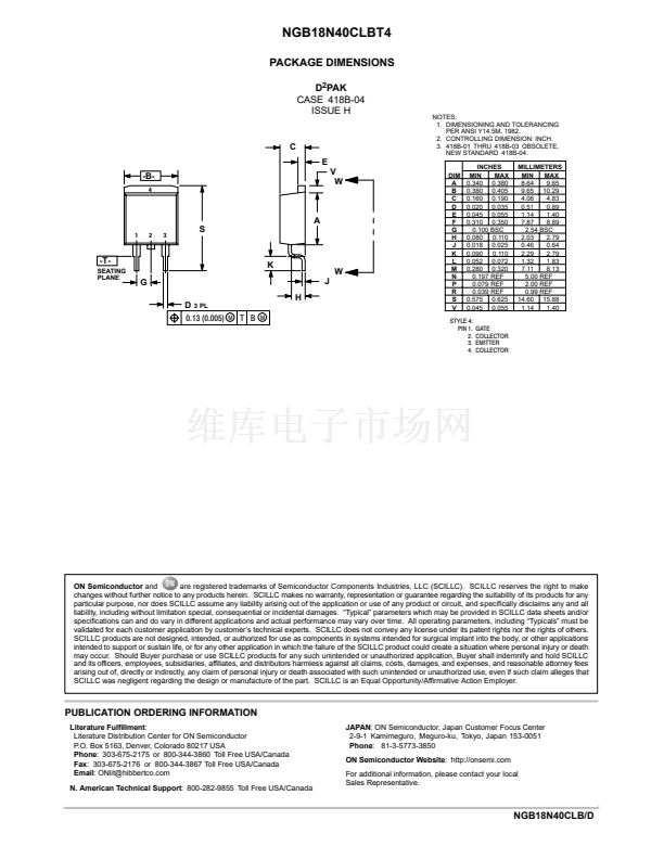
4
2
3
D
2
PAK
CASE 418B
STYLE 4
MARKING
DIAGRAM
4
Collector
GB
18N40B
YWW
GB18N40B = NGB18N40CLB
Y
= Year
WW
= Work Week
ORDERING INFORMATION
Device
NGB18N40CLBT4
Package
D
2
PAK
Shipping
800/Tape & Reel
漏
Semiconductor Components Industries, LLC, 2003
1
March, 2003 - Rev. 0
Publication Order Number:
NGB18N40CLB/D


 1
1
 2
2
 3
3
 4
4
 5
5
 6
6
 7
7
 8
8
