鈥?/div>
HIGH OUTPUT POWER:
15 dBm TYP at 12 GHz
鈥?L
G
= 0.8
碌m,
W
G
= 330
碌m
鈥?LOW PHASE NOISE:
-110 dBc/Hz TYP at 100 KHz offset at f = 12 GHz
鈥?LOW COST PLASTIC PACKAGE
2
NE721S01
OUTLINE DIMENSIONS
(Units in mm)
PACKAGE OUTLINE S01
2.0
鹵
0.2
0
2.
1
J
3
0.65 TYP.
1.9
鹵
0.2
1.6
4
DESCRIPTION
The NE721S01 is a low cost 0.8
碌m
recessed gate GaAs
MESFET, suitable for both amplifier and oscillator applica-
tions. Larger gate geometry make this device ideal for second
and third stages of low noise amplifiers operating in the 1-12
GHz frequency range. The NE721S01 is fabricated with an
epitaxial process resulting in excellent phase noise in oscilla-
tor applications up to 14 GHz. NEC's latest high performance/
low cost plastic packaging technology make the NE721S01
suitable for GPS, TVRO, DBS, PRD and other commercial
applications.
1. Source
2. Drain
3. Source
4. Gate
0.125
鹵
0.05
0.4 MAX
4.0
鹵
0.2
Part Number
Designator (Letter).
When the letter is
upright, the gate lead
is to the right.
ORDERING INFORMATION
PART NUMBER
NE721S01-T1
NE721S01
NE721S01-T1B
QTY
1K/Reel
Bulk up to 4K
4K/Reel
PACKAGE
S01
S01
S01
LEAD
LENGTH
1.0 mm
1.0 mm
1.0 mm
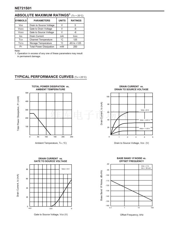
ELECTRICAL CHARACTERISTICS
(T
A
= 25擄C)
PART NUMBER
PACKAGE OUTLINE
SYMBOL
PN
G
S
P
1dB
I
DSS
V
P
g
m
I
GSO
R
TH
PARAMETERS AND CONDITIONS
Phase Noise at V
DS
= 3 V, I
D
= 30 mA, f = 12 GHz, 100 KHz offset
Power Gain at V
DS
= 3 V, I
D
= 30 mA, f = 12 GHz
Output Power at 1 dB Gain Compression Point, f = 12 GHz
V
DS
= 3 V, I
DS
= 30 mA
Saturated Drain Current at V
DS
= 3 V, V
GS
= 0
Pinch Off Voltage at V
DS
= 3 V, I
D
= 100
碌A(chǔ)
Transconductance at V
DS
= 3 V, I
D
= 10 mA
Gate to Source Leak Current at V
GS
= -5 V
Thermal Resistance
UNITS
dBc/Hz
dB
dBm
mA
V
mS
碌A(chǔ)
擄C/W
30
-4.0
20
MIN
NE721S01
S01
TYP
-110
7.0
15.0
60
-2.0
40
1.0
10
300
100
-0.5
MAX
California Eastern Laboratories
1.5 MAX
2.0
鹵
0.2
0.5 TYP.
鹵
0.
2


 1
1
 2
2
 3
3
 4
4
 5
5
