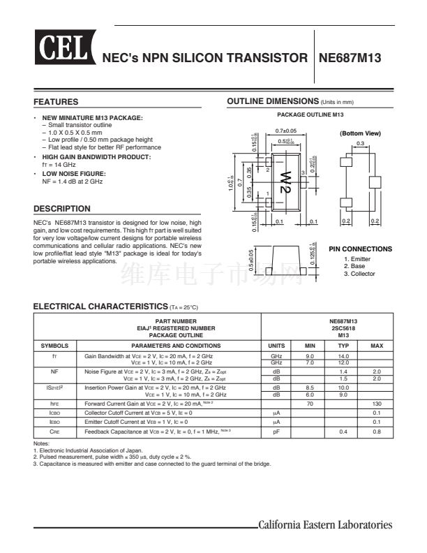
鈥?/div>
0.35
1.0
+0.1
帽0.05
0.7
LOW NOISE FIGURE:
NF = 1.4 dB at 2 GHz
2
3
W2
0.35
1
0.15
+0.1
帽0.05
DESCRIPTION
NEC's NE687M13 transistor is designed for low noise, high
gain, and low cost requirements. This high f
T
part is well suited
for very low voltage/low current designs for portable wireless
communications and cellular radio applications. NEC's new
low profile/flat lead style "M13" package is ideal for today's
portable wireless applications.
0.1
0.1
0.2
0.2
0.125
+0.1
帽0.05
0.5鹵0.05
PIN CONNECTIONS
1. Emitter
2. Base
3. Collector
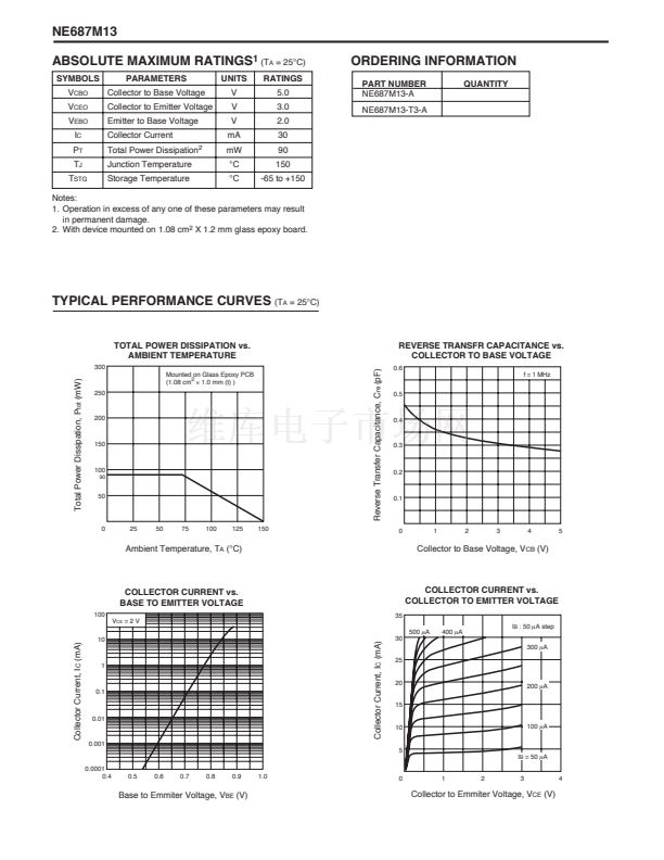
ELECTRICAL CHARACTERISTICS
(T
A
= 25擄C)
EIAJ
1
REGISTERED
SYMBOLS
f
T
NF
|S
21E
|
2
h
FE
I
CBO
I
EBO
C
RE
PART NUMBER
NUMBER
PACKAGE OUTLINE
UNITS
GHz
GHz
dB
dB
dB
dB
碌A(chǔ)
碌A(chǔ)
pF
0.4
8.5
6.0
70
MIN
9.0
7.0
NE687M13
2SC5618
M13
TYP
14.0
12.0
1.4
1.5
10.0
9.0
130
0.1
0.1
0.8
2.0
2.0
MAX
PARAMETERS AND CONDITIONS
Gain Bandwidth at V
CE
= 2 V, I
C
= 20 mA, f = 2 GHz
V
CE
= 1 V, I
C
= 10 mA, f = 2 GHz
Noise Figure at V
CE
= 2 V, I
C
= 3 mA, f = 2 GHz, Z
s
= Z
opt
V
CE
= 1 V, I
C
= 3 mA, f = 2 GHz, Z
s
= Z
opt
Insertion Power Gain at V
CE
= 2 V, I
C
= 20 mA, f = 2 GHz
V
CE
= 1 V, I
C
= 10 mA, f = 2 GHz
Forward Current Gain at V
CE
= 2 V, I
C
= 20 mA,
Note 2
Collector Cutoff Current at V
CB
= 5 V, I
E
= 0
Emitter Cutoff Current at V
EB
= 1 V, I
C
= 0
Feedback Capacitance at V
CB
= 2 V, I
E
= 0, f = 1 MHz,
Note 3
Notes:
1. Electronic Industrial Association of Japan.
2. Pulsed measurement, pulse width
鈮?/div>
350
碌s,
duty cycle
鈮?/div>
2 %.
3. Capacitance is measured with emitter and case connected to the guard terminal of the bridge.
California Eastern Laboratories


 1
1
 2
2
 3
3
 4
4
 5
5
 6
6
 7
7
 8
8
