鈥?/div>
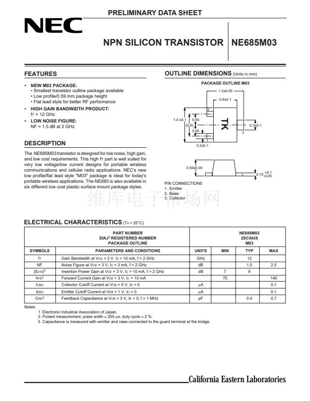
TK
3
1.4 鹵0.1
0.45
(0.9)
0.45
0.3鹵0.1
DESCRIPTION
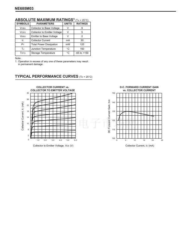
The NE685M03 transistor is designed for low noise, high gain,
and low cost requirements. This high f
T
part is well suited for
very low voltage/low current designs for portable wireless
communications and cellular radio applications. NEC's new
low profile/flat lead style "M03" package is ideal for today's
portable wireless applications. The NE685 is also available in
six different low cost plastic surface mount package styles.
1
0.2鹵0.1
0.59鹵0.05
+0.1
0.15 -0.05
PIN CONNECTIONS
1. Emitter
2. Base
3. Collector
ELECTRICAL CHARACTERISTICS
(T
A
= 25擄C)
EIAJ
1
REGISTERED
SYMBOLS
f
T
NF
|S
21E
|
2
h
FE2
I
CBO
I
EBO
C
RE3
Notes:
1. Electronic Industrial Association of Japan.
2. Pulsed measurement, pulse width
鈮?/div>
350
碌s,
duty cycle
鈮?/div>
2 %.
3. Capacitance is measured with emitter and case connected to the guard terminal at the bridge.
PART NUMBER
NUMBER
PACKAGE OUTLINE
UNITS
GHz
dB
dB
碌A(chǔ)
碌A(chǔ)
pF
0.4
7
75
MIN
NE685M03
2SC5435
M03
TYP
12
1.5
9
140
0.1
0.1
0.7
2.5
MAX
PARAMETERS AND CONDITIONS
Gain Bandwidth at V
CE
= 3 V, I
C
= 10 mA, f = 2 GHz
Noise Figure at V
CE
= 3 V, I
C
= 3 mA, f = 2 GHz
Insertion Power Gain at V
CE
= 3 V, I
C
= 10 mA, f = 2 GHz
Forward Current Gain at V
CE
= 3 V, I
C
= 10 mA
Collector Cutoff Current at V
CB
= 5 V, I
E
= 0
Emitter Cutoff Current at V
EB
= 1 V, I
C
= 0
Feedback Capacitance at V
CB
= 3 V, I
E
= 0, f = 1 MHz
California Eastern Laboratories


 1
1
 2
2
 3
3
