鈥?/div>
TH
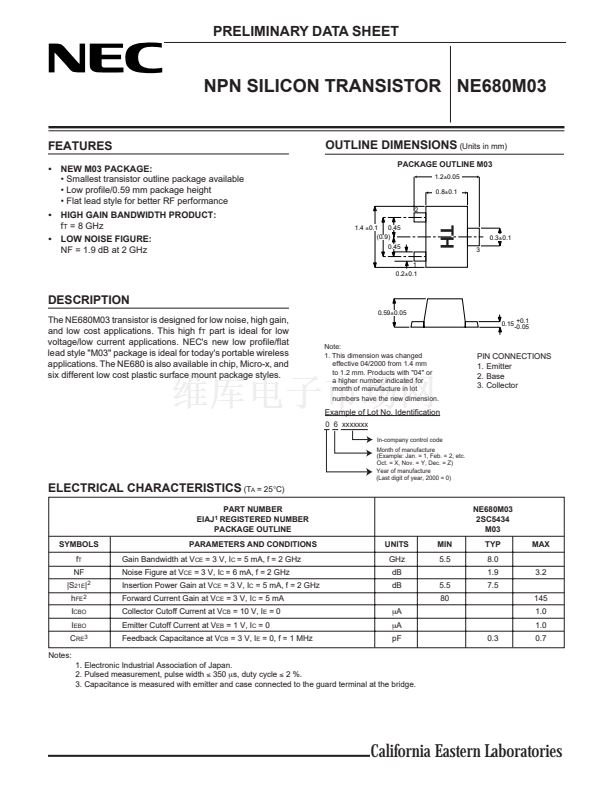
1.4
鹵0.1
0.45
(0.9)
0.45
1
0.2鹵0.1
0.3鹵0.1
3
DESCRIPTION
The NE680M03 transistor is designed for low noise, high gain,
and low cost applications. This high f
T
part is ideal for low
voltage/low current applications. NEC's new low profile/flat
lead style "M03" package is ideal for today's portable wireless
applications. The NE680 is also available in chip, Micro-x, and
six different low cost plastic surface mount package styles.
0.59鹵0.05
+0.1
0.15 -0.05
Note:
1. This dimension was changed
effective 04/2000 from 1.4 mm
to 1.2 mm. Products with "04" or
a higher number indicated for
month of manufacture in lot
numbers have the new dimension.
PIN CONNECTIONS
1. Emitter
2. Base
3. Collector
Example of Lot No. Identification
0 6 xxxxxxx
In-company control code
Month of manufacture
(Example: Jan. = 1, Feb. = 2, etc.
Oct. = X, Nov. = Y, Dec. = Z)
Year of manufacture
(Last digit of year, 2000 = 0)
ELECTRICAL CHARACTERISTICS
(T
A
= 25擄C)
EIAJ
1
REGISTERED
SYMBOLS
f
T
NF
|S
21E
|
2
h
FE2
I
CBO
I
EBO
C
RE3
Notes:
1. Electronic Industrial Association of Japan.
2. Pulsed measurement, pulse width
鈮?/div>
350
碌s,
duty cycle
鈮?/div>
2 %.
3. Capacitance is measured with emitter and case connected to the guard terminal at the bridge.
PART NUMBER
NUMBER
PACKAGE OUTLINE
UNITS
GHz
dB
dB
碌A
碌A
pF
0.3
5.5
80
MIN
5.5
NE680M03
2SC5434
M03
TYP
8.0
1.9
7.5
145
1.0
1.0
0.7
3.2
MAX
PARAMETERS AND CONDITIONS
Gain Bandwidth at V
CE
= 3 V, I
C
= 5 mA, f = 2 GHz
Noise Figure at V
CE
= 3 V, I
C
= 6 mA, f = 2 GHz
Insertion Power Gain at V
CE
= 3 V, I
C
= 5 mA, f = 2 GHz
Forward Current Gain at V
CE
= 3 V, I
C
= 5 mA
Collector Cutoff Current at V
CB
= 10 V, I
E
= 0
Emitter Cutoff Current at V
EB
= 1 V, I
C
= 0
Feedback Capacitance at V
CB
= 3 V, I
E
= 0, f = 1 MHz
California Eastern Laboratories


 1
1
 2
2
 3
3
