Philips Semiconductors
Product specification
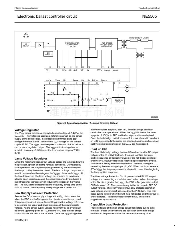
Electronic ballast controller circuit
NE5565
DESCRIPTION
The Electronic Ballast controller chip has been designed in a bipolar
process. It is housed in a 20-lead dual-in-line plastic package. The
control chip contains the equivalent of two (2) switched mode power
supply control circuits. The first SMPS controller is a DC-to-DC
converter operating in the discontinuous current conduction mode.
It is used as a PFC in the ballast system to provide a DC voltage
step-up function, good AC power factor, low AC current harmonic
distortion, and circuit protection against some types of AC voltage
transients. The PFC uses pulse width modulation to control the
power transfer with an external MOS power transistor. The second
SMPS circuit is a half-bridge oscillator circuit. It converts the DC
output voltage of the PFC into a high frequency AC voltage for
operating lamps. Power transfer in this circuit is controlled by
changing the switch frequency. The half-bridge controller circuit is
capable of driving two external high voltage MOS power transistors
and it has circuits to regulate the lamp current, limit the peak lamp
voltage, and protect the power switches during fault conditions. This
electronic ballast controller circuit has the capability of being used in
a dimming application.
PIN CONFIGURATION
N Package
C
T
C
P
1
2
20
DC
OUT
19
DC
18
OV
17
PF
16
V
REF
15
I
PRIM
14
OUT
H
13
V
CC
12
OUT
P
11
GND
D
MAX
3
R
T
RXCX
4
5
V
LAMP
6
C
RECT
7
LI2
8
LI
9
CSI
10
SL00524
Figure 1. Pin Configuration
FEATURES:
鈥?/div>
Complete PFC correction and dimming ballast control on one IC
鈥?/div>
Low line current distortion PFC
ORDERING INFORMATION
DESCRIPTION
20-Pin Plastic Dual-In-Line Package (DIP)
鈥?/div>
Selectable variable frequency modes
鈥?/div>
Programmable pre-hit and ignition
鈥?/div>
Lamp over-voltage protection
鈥?/div>
PFC over-voltage protection for preventing over-shooting due to
load removal
TEMPERATURE RANGE
0 to +85
擄
C
ORDER CODE
NE5565N
DWG #
SOT146-1
BLOCK DIAGRAM
V
LAMP
RXCX
6
5
4
V
CC
C
RECT
LI2
LI
7
8
9
3
D
MAX
C
P
C
T
R
T
CSI
10
2
1
GND
11
12
20 DC
OUT
OUT
P
V
CC
13
14
OUT
H
15
I
PRIM
16
V
REF
17 18
PF OV
19
DC
SL00525
Figure 2. Block Diagram
1996 May 21
1
853-1835 16843
NE5565N相關(guān)型號PDF文件下載
-
型號
版本
描述
廠商
下載
-
英文版
PRECISION TIMERS
-
英文版
Timers for Timing Delays and Oscillator Application in Comme...
-
英文版
Single Timer
FAIRCHILD
-
英文版
Precision Timer
WINGS
-
英文版
PRECISION TIMERS
TI
-
英文版
GENERAL PURPOSE SINGLE BIPOLAR TIMERS
-
英文版
Timer
PHILIPS
-
英文版
Philips Semiconductors Linear Products Product specification...
-
英文版
1
2
3
4
8
7
6
5
GND
TRIG
OUT
RESET
V
CC
DISCH
THRES
CONT
3 2...
-
英文版
GENERAL PURPOSE SINGLE BIPOLAR TIMERS
STMICROELECTRON...
-
英文版
PRECISION TIMERS
NEC [NEC]
-
英文版
PRECISION TIMERS
TI [Texas ...
-
英文版
Precision Timer
WINGS [Win...
-
英文版
Single Timer
FAIRCHILD ...
-
英文版
Timers for Timing Delays and Oscillator Application in Comme...
HARRIS [Ha...
-
英文版
Timer
PHILIPS [P...
-
英文版
Dual Timer
FAIRCHILD
-
英文版
DUAL PRECISION TIMERS
TI
-
英文版
GENERAL PURPOSE DUAL BIPOLAR TIMERS
-
英文版
Dual timer
PHILIPS


 1
1
 2
2
 3
3
 4
4
 5
5
 6
6
