鈥?/div>
Power Range: -30 dBm to 20 dBm
Includes Input Matching Circuit
Internal Temperature Compensation
Wide Input Frequency Range: 100 MHz to 3.0 GHz
Direct Connection to Battery: 2.7 to 4.8 V
Reference Signal Output
TSOP-6 Package or Bare Die
Global System for Mobile Communication (GSM/DCS/PCS)
Dual/Triple Band TDMA/EDGE and GPRS
Personal Communication Network (PCN)
Power Amplifier Modules
xxx = Specific Device Code
M = Date Code
Typical Applications
PIN CONNECTIONS
DET
V
CC
EN
1
2
3
(Top View)
6
5
4
REF
GND
RF_IN
V
CC
ORDERING INFORMATION
V
CC
RF
RF_IN
DET
DETECTED
VOLTAGE
REFERENCE
VOLTAGE
TBD
Device
Package
TSOP-6
Shipping
TBD
ENABLE
EN
GND
REF
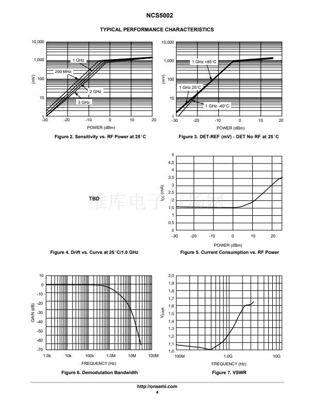
Figure 1.
This document contains information on a product under development. ON Semiconductor
reserves the right to change or discontinue this product without notice.
漏
Semiconductor Components Industries, LLC, 2003
1
February, 2003 - Rev. 0
Publication Order Number:
NCS5002/D


 1
1
 2
2
 3
3
 4
4
 5
5
 6
6
