NCP5201
Dual Output
DDR Power Controller
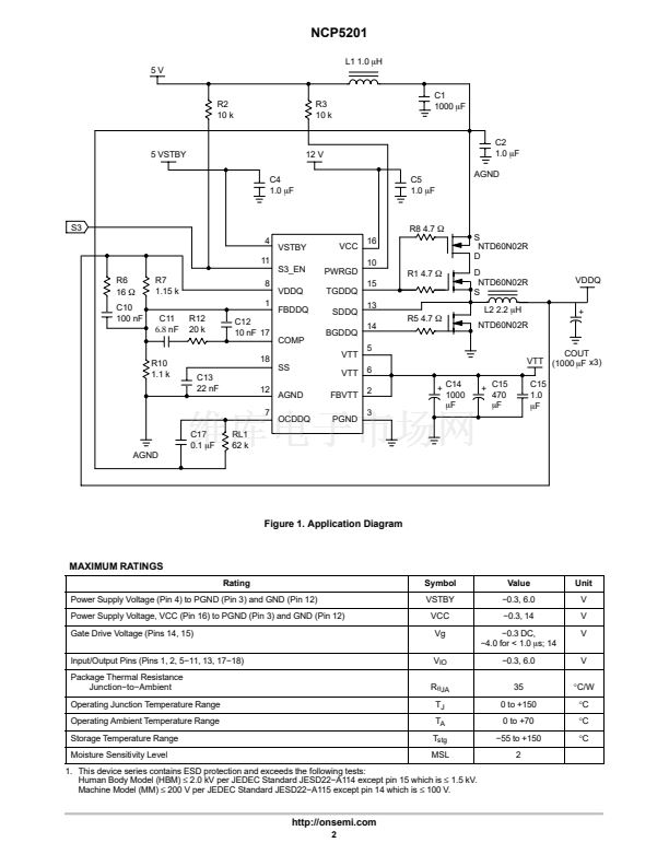
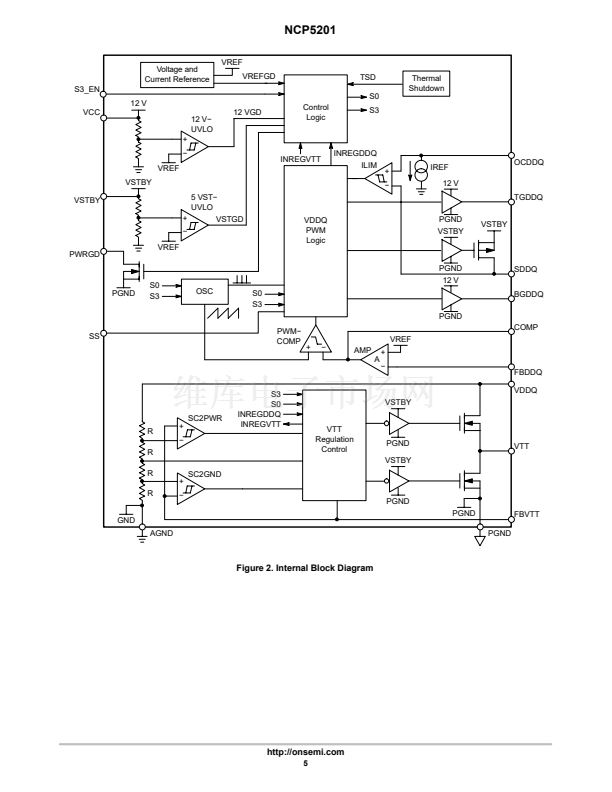
The NCP5201 Dual DDR Power Controller is specifically
designed as a total power solution for a high current DDR memory
system. This IC combines the efficiency of a PWM controller for the
VDDQ supply with the simplicity of a linear regulator for the VTT
memory termination voltage. The secondary regulator (VTT) is
designed to automatically track at half the primary regulator voltage
(VDDQ). An internal power good voltage monitor tracks both
VDDQ and VTT outputs and notifies the user in the event of a fault
on either output. Protective features include soft start circuitry,
undervoltage monitoring of VCC and VSTBY, and thermal
shutdown. The IC is packaged in a 5
脳
6 QFN鈭?8.
Features
http://onsemi.com
MARKING
DIAGRAM
1
1
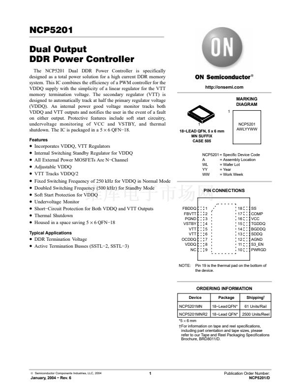
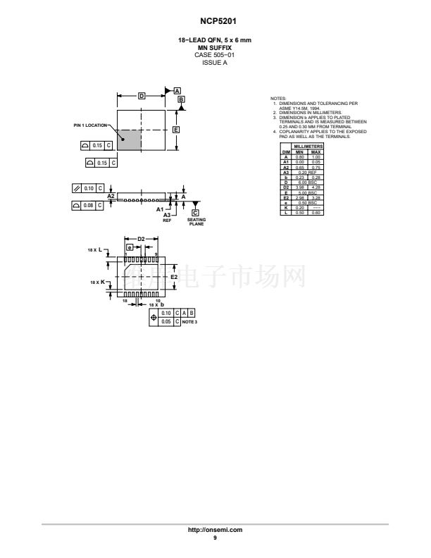
18鈭扡EAD QFN, 5 x 6 mm
MN SUFFIX
CASE 505
NCP5201
AWLYYWW
鈥?/div>
鈥?/div>
鈥?/div>
鈥?/div>
鈥?/div>
鈥?/div>
鈥?/div>
鈥?/div>
鈥?/div>
鈥?/div>
鈥?/div>
鈥?/div>
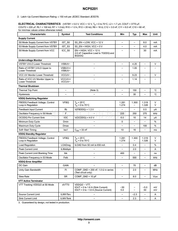
Incorporates VDDQ, VTT Regulators
Internal Switching Standby Regulator for VDDQ
All External Power MOSFETs Are N鈭扖hannel
Adjustable VDDQ
VTT Tracks VDDQ/2
Fixed Switching Frequency of 250 kHz for VDDQ in Normal Mode
Doubled Switching Frequency (500 kHz) for Standby Mode
Soft Start Protection for VDDQ
Undervoltage Monitor
Short鈭扖ircuit Protection for Both VDDQ and VTT Outputs
Thermal Shutdown
Housed in a space saving 5
脳
6 QFN鈭?8
NCP5201 = Specific Device Code
A
= Assembly Location
WL
= Wafer Lot
YY
= Year
WW
= Work Week
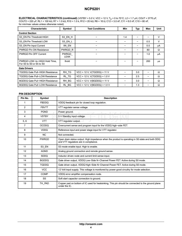
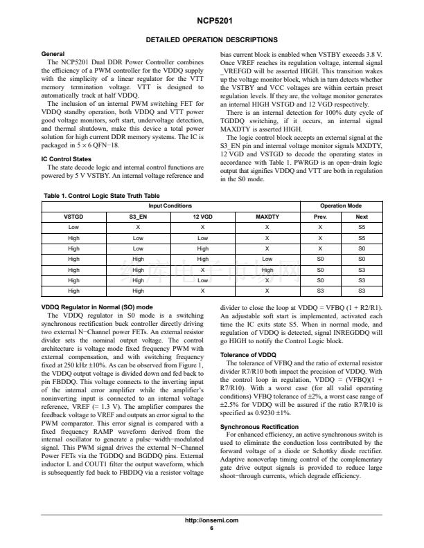
PIN CONNECTIONS
Typical Applications
鈥?/div>
DDR Termination Voltage
鈥?/div>
Active Termination Busses (SSTL鈭?, SSTL鈭?)
FBDDQ
FBVTT
PGND
VSTBY
VTT
VTT
OCDDQ
VDDQ
NC
1
2
3
4
5
6
7
8
9
18
17
16
15
14
13
12
11
10
SS
COMP
VCC
TGDDQ
BGDDQ
SDDQ
AGND
S3_EN
PWRGD
NOTE:
Pin 19 is the thermal pad on the bottom of
the device.
ORDERING INFORMATION
Device
NCP5201MN
NCP5201MNR2
Package
18鈭扡ead QFN*
18鈭扡ead QFN*
Shipping
鈥?/div>
61 Units/Rail
2500 Units/Reel
*5
脳
6 mm
鈥燜or information on tape and reel specifications,
including part orientation and tape sizes, please
refer to our Tape and Reel Packaging Specifications
Brochure, BRD8011/D.
漏
Semiconductor Components Industries, LLC, 2004
1
January, 2004 鈭?Rev. 6
Publication Order Number:
NCP5201/D
NCP5201/D相關(guān)型號PDF文件下載
-
型號
版本
描述
廠商
下載
-
英文版
150 mA CMOS Low Noise Low-Dropout Voltage Regulator
ONSEMI
-
英文版
Monolithic High Voltage Gated Oscillator Power Switching Reg...
-
英文版
80 mA CMOS Low Iq Voltage Regulator in an SC70−5
ONSEMI
-
英文版
80 mA CMOS Low IqVoltage Regulator in anSC70-5
-
英文版
150 mA CMOS Low Iq Low-Dropout Voltage Regulator
ONSEMI
-
英文版
150 mA CMOS Low IqLow-Dropout VoltageRegulator
-
英文版
80 mA CMOS Low Iq Voltage Regulator in an SC70-5
ONSEMI
-
英文版
Supervisory IC for Desktop Power Supply Monitoring
-
英文版
150 mA CMOS Low Iq Low-Dropout Voltage Regulator
ONSEMI
-
英文版
-
英文版
-
英文版
80 mA CMOS Low Iq NOCAP Voltage Regulator
ONSEMI
-
英文版
-
英文版
-
英文版
150 mA CMOS Low Iq Low-Dropout Voltage Regulator
ONSEMI
-
英文版
150 mA CMOS Low Iq Low-Dropout Voltage Regulator
ONSEMI [ON...
-
英文版
80 mA CMOS Low Iq Low-Dropout Voltage Regulator
ONSEMI
-
英文版
80 mA CMOS Low Iq Low-Dropout Voltage Regulator
ONSEMI [ON...
-
英文版
80 mA CMOS Low Iq Low-Dropout Voltage Regulator
ONSEMI
-
英文版
80 mA CMOS Low Iq Low-Dropout Voltage Regulator
ONSEMI [ON...


 1
1
 2
2
 3
3
 4
4
 5
5
 6
6
 7
7
 8
8
 9
9
 10
10
