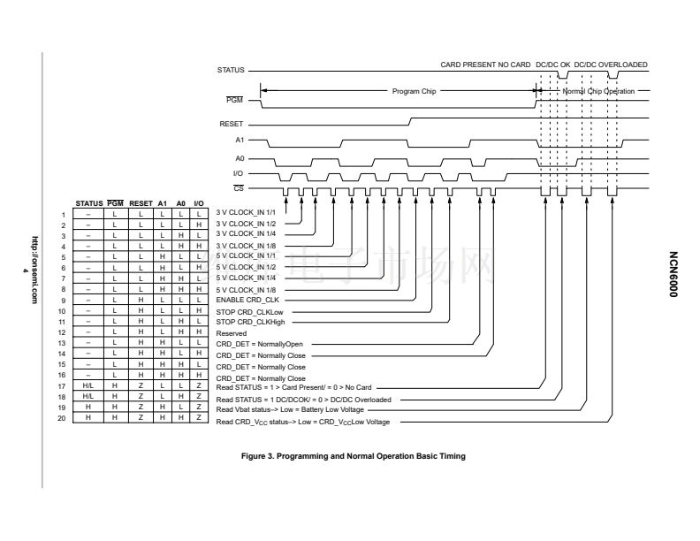
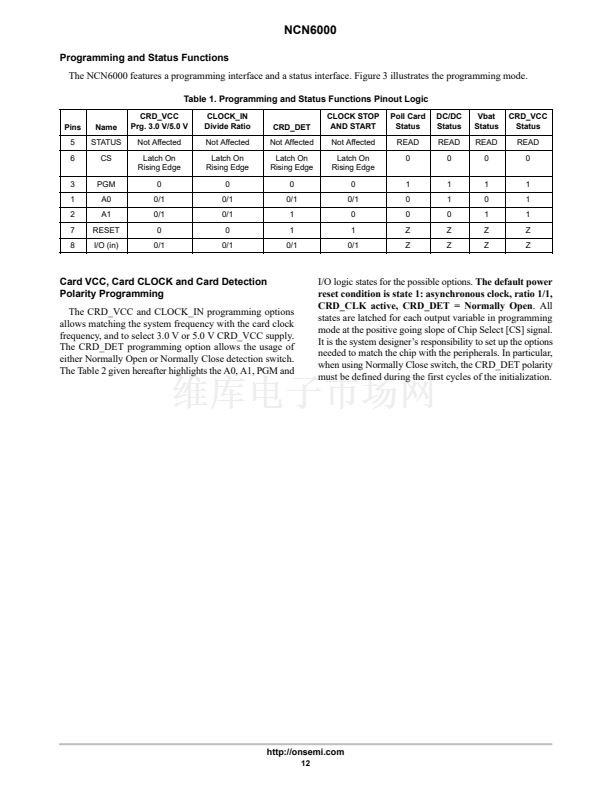
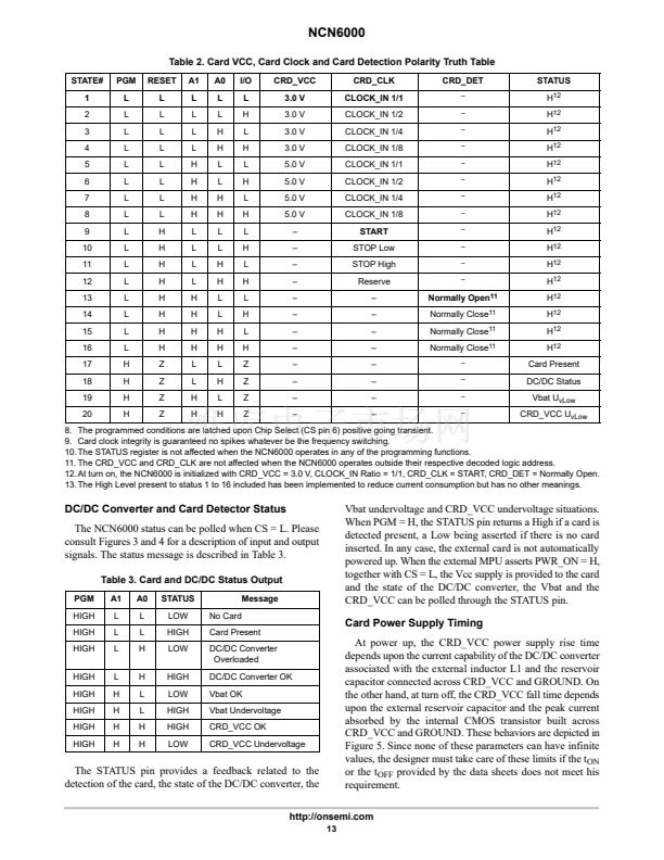
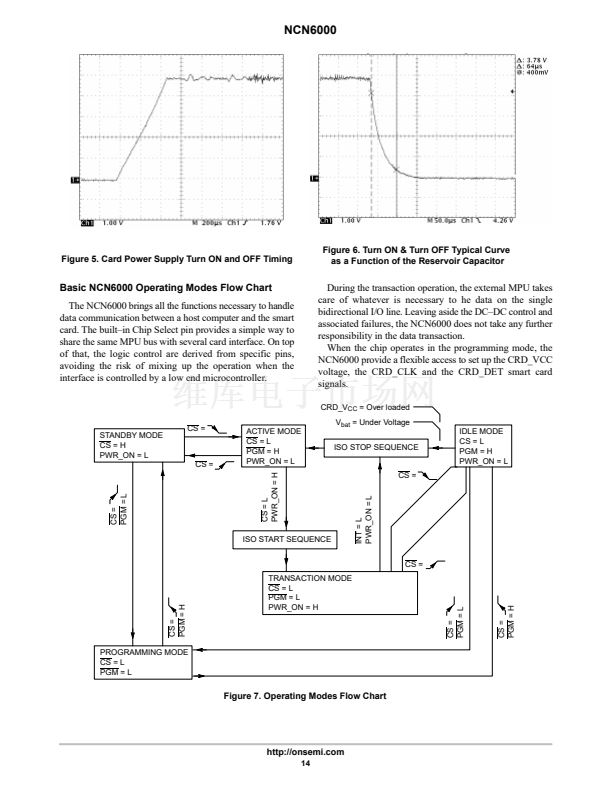
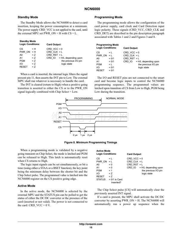
鈥?/div>
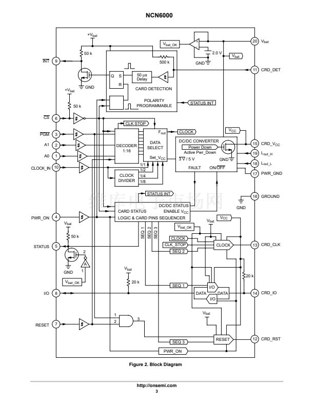
Operation
Built鈥搃n DC/DC Converter Generates the Vcc Supply with a Single
External Low Cost Inductor only, providing a High Efficiency Power
Conversion
Full Control of the Power Up/Down Sequence Yields High Signal
Integrity on both the Card I/O and the Signal Lines
Programmable Card Clock Generator
Built鈥搃n Chip Select Logic allows Parallel Coupling Operation
ESD Protection on Card Pins (4.0 kV, Human Body Model)
Fault Monitoring includes Vbat
low
and Vcc
low,
providing Logic
Feedback to External CPU
Card Detection Programmable to Handle Positive or Negative Going
Input
Built鈥搃n Programmable CRD_CLK Stop Function Handle both High
or Low State
20
1
A
WL, L
YY, Y
WW, W
= Assembly Location
= Wafer Lot
= Year
= Work Week
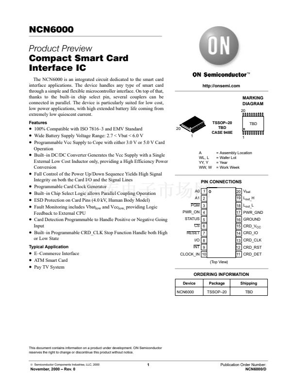
PIN CONNECTIONS
A0 1
A1 2
PGM 3
PWR_ON 4
STATUS 5
CS 6
RESET 7
I/O 8
INT 9
CLOCK_IN 10
(Top View)
20 V
bat
19 L
out_
H
18 L
out_
L
17 PWR_GND
16 GROUND
15 CRD_V
CC
14 CRD_IO
13 CRD_CLK
12 CRD_RST
11 CRD_DET
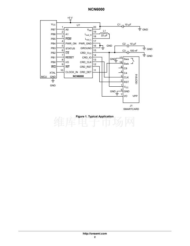
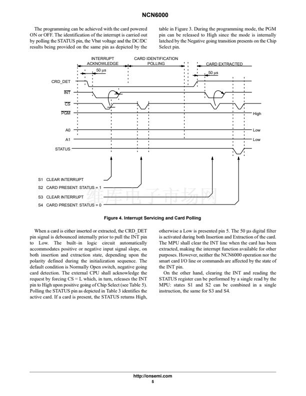
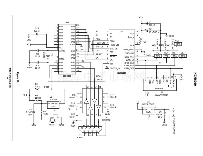
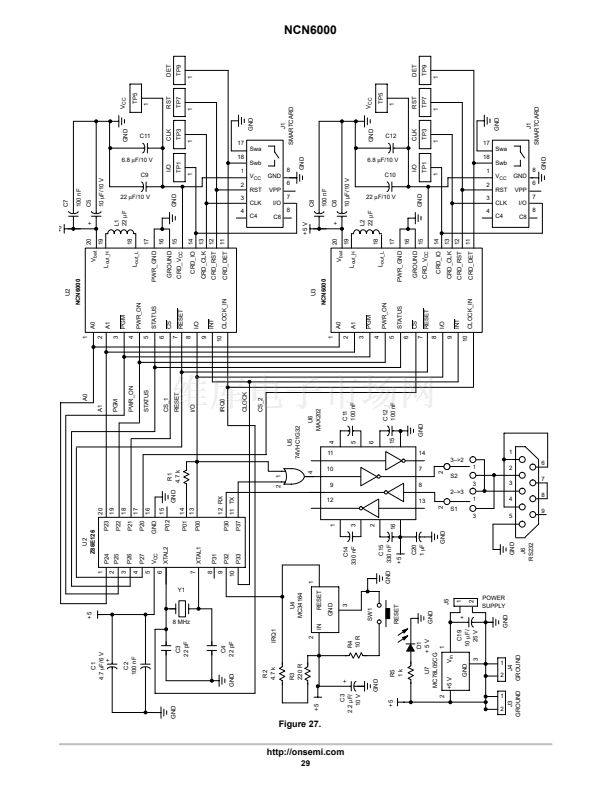
Typical Application
鈥?/div>
E鈥揅ommerce Interface
鈥?/div>
ATM Smart Card
鈥?/div>
Pay TV System
ORDERING INFORMATION
Device
NCN6000
Package
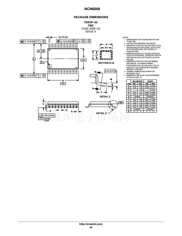
TSSOP鈥?0
Shipping
TBD
This document contains information on a product under development. ON Semiconductor
reserves the right to change or discontinue this product without notice.
漏
Semiconductor Components Industries, LLC, 2000
1
November, 2000 鈥?Rev. 0
Publication Order Number:
NCN6000/D


 1
1
 2
2
 3
3
 4
4
 5
5
 6
6
 7
7
 8
8
 9
9
 10
10
 11
11
 12
12
 13
13
 14
14
 15
15
 16
16
 17
17
 18
18
 19
19
 20
20
 21
21
 22
22
 23
23
 24
24
 25
25
 26
26
 27
27
 28
28
 29
29
 30
30
 31
31
 32
32
