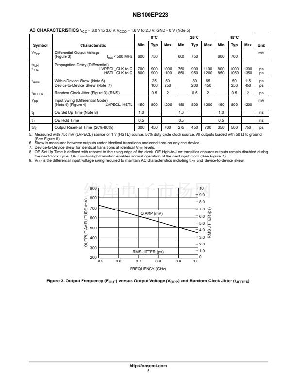
NB100EP223
3.3V 1:22 Differential
HSTL/PECL to HSTL Clock
Driver with LVTTL Clock
Select and Output Enable
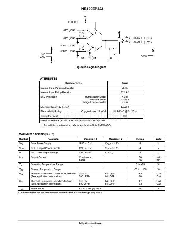
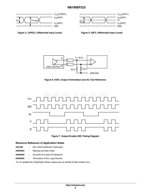
The NB100EP223 is a low skew 1-to-22 differential clock driver,
designed with clock distribution in mind, accepting two clock sources
into an input multiplexer. The part is designed for use in low voltage
applications which require a large number of outputs to drive precisely
aligned low skew signals to their destination. The two clock inputs are
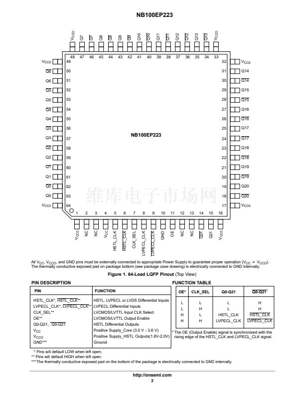
differential HSTL or LVPECL and they are selected by the CLK_SEL
pin which is LVTTL. To avoid generation of a runt clock pulse when
the device is enabled/disabled, the Output Enable (OE), which is
LVTTL, is synchronous ensuring the outputs will only be
enabled/disabled when they are already in LOW state (See Figure 7).
The NB100EP223 guarantees low output-to-output skew. The
optimal design, layout, and processing minimize skew within a device
and from lot to lot. In any differential output pair, the same bias and
termination scheme is required. Unused output pairs should be left
unterminated (open) to 鈥渞educe power and switching noise as much as
possible.鈥?Any unused single line of a differential pair should be
terminated the same as the used line to maintain balanced loads on the
differential driver outputs. The output structure uses an open emitter
architecture and will be terminated with 50
W
to ground instead of a
standard HSTL configuration (See Figure 6). The wide VIHCMR
specification allows both pair of CLOCK inputs to accept LVDS
levels.
http://onsemi.com
MARKING
DIAGRAM*
64
1
64
1
NB100
EP223
AWLYYWW
64-LEAD LQFP
CASE 848G
THERMALLY ENHANCED
FA SUFFIX
A
WL
YY
WW
= Assembly Location
= Wafer Lot
= Year
= Work Week
*For additional information, see Application Note
AND8002/D
鈥?/div>
100 ps Typical Device-to- Device Skew
鈥?/div>
25 ps Typical Within Device Skew
鈥?/div>
HSTL Compatible Outputs Drive 50
W
to Ground With No
Offset Voltage
鈥?/div>
Maximum Frequency >500 MHz
ORDERING INFORMATION
Device
NB100EP223FA
NB100EP223FAR2
Package
LQFP-64
Shipping
160 Units/Tray
鈥?/div>
1 ns Typical Propagation Delay
鈥?/div>
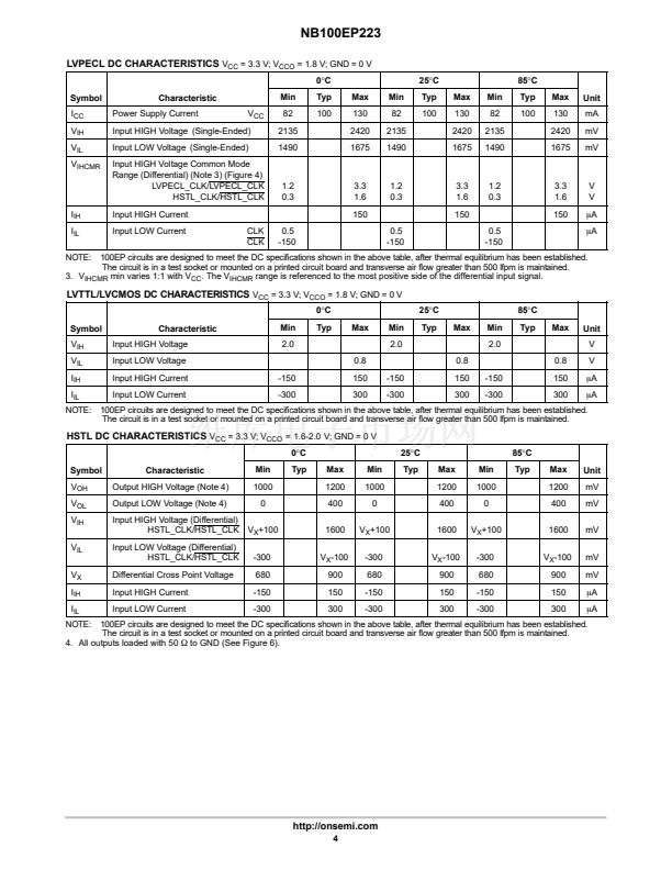
LVPECL and HSTL Mode Operating Range: V
CC
= 3 V to 3.6 V
with GND = 0 V, V
CCO
= 1.6 V to 2.0 V
鈥?/div>
Q Output will Default Low with Inputs Open
LQFP-64 1500/Tape & Reel
鈥?/div>
Thermally Enhanced 64-Lead LQFP
鈥?/div>
CLOCK Inputs are LVDS-Compatible; Requires External 100
W
LVDS Termination Resistor
漏
Semiconductor Components Industries, LLC, 2003
1
June, 2003 - Rev. 5
Publication Order Number:
NB100EP223/D
NB100EP223/D相關(guān)型號(hào)PDF文件下載
-
型號(hào)
版本
描述
廠商
下載
-
英文版
CHIP LED DEVICE
SEOUL [Seoul Se...
-
英文版
CHIP LED DEVICE
SEOUL [Seoul Se...
-
英文版
BAG NOTEBOOK NYLON TOP-LOAD
-
英文版
BAG NOTEBOOK NYLON TOP-LOAD
-
英文版
BAG NOTEBOOK NYLON TOP-LOAD
-
英文版
BAG NOTEBOOK LEATHER TOP-LOAD
-
英文版
BAG NOTEBOOK LEATHER TOP-LOAD
-
英文版
BAG NOTEBOOK LEATHER TOP-LOAD
-
英文版
BAG NOTEBOOK NYLON W/WHEELS
-
英文版
BAG BACKPACK NYLON TOP-LOAD
-
英文版
BAG BACKPACK NYLON TOP-LOAD
-
英文版
3.3V�1:22 Differential HSTL/PECL to HSTL Clock Driver with L...
ONSEMI
-
英文版
3.3V 1:22 Differential HSTL/PECL to HSTL Clock Driver with L...
-
英文版
3.3V Dual Differential LVPECL/LVDS to LVTTL Translator
ONSEMI
-
英文版
3.3V Dual Differential LVPECL/LVDS to LVTTL Translator
ONSEMI [ON...
-
英文版
2.5V / 3.3V Quad Differential Driver/Receiver
ONSEMI
-
英文版
2.5V / 3.3V ECL Quad Differential Driver/Receiver
-
英文版
2.5V / 3.3V / 5V�ECL Dual Differential 2:1 Multiplexer
ONSEMI
-
英文版
2.5V / 3.3V / 5V�ECL Dual Differential 2:1 Multiplexer
ONSEMI [ON...
-
英文版
2.5V / 3.3V Any Level Positive Input to -2.5V -3.3V / -5V NE...
ONSEMI


 1
1
 2
2
 3
3
 4
4
 5
5
 6
6
 7
7
 8
8
 9
9
 10
10
