MOTOROLA
The RF Line
SEMICONDUCTOR TECHNICAL DATA
Freescale Semiconductor, Inc.
Order this document
by MW4IC915/D
RF LDMOS Wideband Integrated
Power Amplifiers
The MW4IC915MB/GMB wideband integrated circuit is designed for GSM
and GSM EDGE base station applications. It uses Motorola鈥檚 newest High
Voltage (26 to 28 Volts) LDMOS IC technology and integrates a multi-stage
structure. Its wideband On Chip design makes it usable from 750 to 1000 MHz.
The linearity performances cover all modulations for cellular applications: GSM,
GSM EDGE, TDMA, N-CDMA and W-CDMA.
鈥?/div>
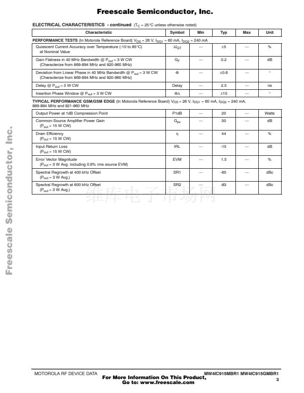
Typical GSM/GSM EDGE Performances: 26 Volts, I
DQ1
= 60 mA, I
DQ2
=
240 mA, 869-894 MHz and 921-960 MHz
Output Power 鈥?3 Watts Avg.
Power Gain 鈥?31 dB
Efficiency 鈥?19%
Spectral Regrowth @ 400 kHz Offset = -65 dBc
Spectral Regrowth @ 600 kHz Offset = -83 dBc
EVM 鈥?1.5%
鈥?/div>
Typical Performance: 860-960 MHz, 26 Volts
Output Power 鈥?15 Watts CW
Power Gain 鈥?30 dB
Efficiency 鈥?44%
鈥?/div>
On Chip Matching (50 Ohm Input, >3 Ohm Output)
鈥?/div>
Integrated Temperature Compensation Capability with Enable/Disable
Function
鈥?/div>
Integrated ESD Protection
鈥?/div>
Capable of Handling 5:1 VSWR, @ 26 Vdc, f = 921 MHz,
P
out
= 15 W CW, I
DQ1
= 90 mA, I
DQ2
= 240 mA
鈥?/div>
Can Be Bolted or Soldered through a Hole in the Circuit Board for
Maximum Thermal Performance
鈥?/div>
Also Available in Gull Wing for Surface Mount
鈥?/div>
In Tape and Reel. R1 Suffix = 500 Units per 44 mm, 13 inch Reel.
MW4IC915MBR1
MW4IC915GMBR1
GSM/GSM EDGE,
N-CDMA, W-CDMA
860 - 960 MHz, 15 W, 26 V
RF LDMOS WIDEBAND
INTEGRATED POWER AMPLIFIERS
Freescale Semiconductor, Inc...
CASE 1329-09
TO-272 WB-16
PLASTIC
MW4IC915MBR1
CASE 1329A-03
TO-272 WB-16 GULL
PLASTIC
MW4IC915GMBR1
PIN CONNECTIONS
V
DS1
RF
in
RF
out
/V
DS2
GND
NC
NC
V
DS1
NC
RF
in
V
GS1
V
GS2
Temperature Compensation
NC
V
GS1
V
GS2
NC
GND
1
2
3
4
5
6
7
8
9
10
11
16
15
GND
NC
14
RF
out
/
V
DS2
Functional Block Diagram
13
12
NC
GND
(Top View)
REV 2
MOTOROLA RF
錚?/div>
Motorola, Inc. 2003
DEVICE DATA
For More Information On This Product,
Go to: www.freescale.com
MW4IC915MBR1 MW4IC915GMBR1
1
MW4IC915相關(guān)型號PDF文件下載
-
型號
版本
描述
廠商
下載
-
英文版
MW4IC915MBR1. MW4IC915GMBR1 GSM/GSM EDGE. N-CDMA. W-CDMA. 86...
ETC
-
英文版
RF LDMOS Wideband Integrated Power Amplifiers
FREESCALE
-
英文版
MW4IC001NR4 800-2170 MHz, 900 mW, 28 V W-CDMA RF LDMOS Wideb...
-
英文版
RF LDMOS Wideband Integrated Power Amplifiers
-
英文版
RF LDMOS Wideband Integrated Power Amplifiers
MOTOROLA [...
-
英文版
RF LDMOS Wideband Integrated Power Amplifiers
-
英文版
RF LDMOS Wideband Integrated Power Amplifiers
MOTOROLA [...
-
英文版
MW4IC915NBR1, MW4IC915GNBR1 860-960 MHz, 15 W, 26 V GSM/GSM ...
-
英文版
RF LDMOS Wideband Integrated Power Amplifiers
-
英文版
RF LDMOS Wideband Integrated Power Amplifiers
MOTOROLA [...
-
英文版
MW4IC2020NBR1, MW4IC2020GNBR1 1805-1990 MHz, 20 W, 26 V, GSM...
-
英文版
MW4IC2230NBR1, MW4IC2230GNBR1 2110-2170 MHz, 30 W, 28 V Sing...
-
英文版
MW4IC001MR4 800-2170 MHz. 900 mW. 28 V. W-CDMA. RF LDMOS Wid...
ETC
-
英文版
W-CDMA 0.8-2.17 GHz, 900 mW, 28 V RF LDMOS Wideband Integrat...
-
英文版
W-CDMA 0.8-2.17 GHz, 900 mW, 28 V RF LDMOS Wideband Integrat...
-
英文版
RF LDMOS Wideband Integrated Power Amplifiers
FREESCALE
-
英文版
RF LDMOS Wideband Integrated Power Amplifiers
-
英文版
RF LDMOS Wideband Integrated Power Amplifiers
FREESCALE
-
英文版
RF LDMOS WIDEBAND INTEGRATED POWER AMPLIFIERS
MOTOROLA [...
-
英文版
RF LDMOS Wideband Integrated Power Amplifiers
MOTOROLA [...


 1
1
 2
2
 3
3
 4
4
 5
5
 6
6
 7
7
 8
8
 9
9
 10
10
 11
11
 12
12
 13
13
 14
14
 15
15
 16
16
