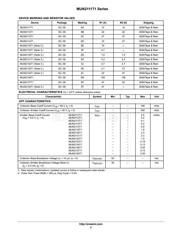
MUN2111T1 Series
Preferred Devices
Bias Resistor Transistors
PNP Silicon Surface Mount Transistors
with Monolithic Bias Resistor Network
This new series of digital transistors is designed to replace a single
device and its external resistor bias network. The BRT (Bias Resistor
Transistor) contains a single transistor with a monolithic bias network
consisting of two resistors; a series base resistor and a base鈥揺mitter
resistor. The BRT eliminates these individual components by
integrating them into a single device. The use of a BRT can reduce
both system cost and board space. The device is housed in the SC鈥?9
package which is designed for low power surface mount applications.
http://onsemi.com
PIN 3
COLLECTOR
(OUTPUT)
R1
PIN 2
BASE
(INPUT)
R2
鈥?/div>
鈥?/div>
鈥?/div>
鈥?/div>
鈥?/div>
Simplifies Circuit Design
Reduces Board Space
Reduces Component Count
Moisture Sensitivity Level: 1
ESD Rating 鈥?Human Body Model: Class 1
ESD Rating
鈥?Machine Model: Class B
鈥?/div>
The SC鈥?9 package can be soldered using wave or reflow.
The modified gull鈥搘inged leads absorb thermal stress during
soldering eliminating the possibility of damage to the die.
鈥?/div>
Available in 8 mm embossed tape and reel
Use the Device Number to order the 7 inch/3000 unit reel.
MAXIMUM RATINGS
(T
A
= 25擄C unless otherwise noted)
Rating
Collector-Base Voltage
Collector-Emitter Voltage
Collector Current
Symbol
V
CBO
V
CEO
I
C
Value
50
50
100
Unit
Vdc
Vdc
mAdc
PIN 1
EMITTER
(GROUND)
3
2
1
SC鈥?9
CASE 318D
PLASTIC
MARKING DIAGRAM
6x
6x = Device Code
x = A 鈥?T*
THERMAL CHARACTERISTICS
Characteristic
Total Device Dissipation
T
A
= 25擄C
Derate above 25擄C
Thermal Resistance 鈥?/div>
Junction-to-Ambient
Thermal Resistance 鈥?/div>
Junction-to-Lead
Junction and Storage
Temperature Range
1. FR鈥? @ Minimum Pad
2. FR鈥? @ 1.0 x 1.0 inch Pad
Symbol
P
D
Max
230 (Note 1.)
338 (Note 2.)
1.8 (Note 1.)
2.7 (Note 2.)
540 (Note 1.)
370 (Note 2.)
264 (Note 1.)
287 (Note 2.)
鈥?5 to +150
Unit
mW
擄C/W
擄C/W
擄C/W
擄C
ORDERING INFORMATION
See detailed ordering and shipping information on page 2 of
this data sheet.
DEVICE MARKING INFORMATION
*See device marking table on page 2 of this data sheet.
Preferred
devices are recommended choices for future use
and best overall value.
R
胃JA
R
胃JL
T
J
, T
stg
漏
Semiconductor Components Industries, LLC, 2001
March, 2001 鈥?Rev. 11
Publication Order Number:
MUN2111T1/D
MUN2111T1/D相關(guān)型號PDF文件下載
-
型號
版本
描述
廠商
下載
-
英文版
Bias Resistor Transistor
ONSEMI
-
英文版
Bias Resistor Transistor
ONSEMI [ON...
-
英文版
NPN SILICON BIAS RESISTOR TRANSISTOR
ONSEMI
-
英文版
NPN SILICON BIAS RESISTOR TRANSISTOR
ONSEMI [ON...
-
英文版
NPN SILICON BIAS RESISTOR TRANSISTOR
ONSEMI
-
英文版
NPN SILICON BIAS RESISTOR TRANSISTOR
ONSEMI [ON...
-
英文版
NPN SILICON BIAS RESISTOR TRANSISTOR
ONSEMI
-
英文版
NPN SILICON BIAS RESISTOR TRANSISTOR
ONSEMI [ON...
-
英文版
NPN SILICON BIAS RESISTOR TRANSISTOR
ONSEMI
-
英文版
NPN SILICON BIAS RESISTOR TRANSISTOR
ONSEMI [ON...
-
英文版
NPN SILICON BIAS RESISTOR TRANSISTOR
ONSEMI
-
英文版
NPN SILICON BIAS RESISTOR TRANSISTOR
ONSEMI [ON...
-
英文版
NPN SILICON BIAS RESISTOR TRANSISTOR
ONSEMI
-
英文版
Bias Resistor Transistor
LRC
-
英文版
NPN SILICON BIAS RESISTOR TRANSISTOR
-
英文版
NPN SILICON BIAS RESISTOR TRANSISTOR
ONSEMI [ON...
-
英文版
NPN SILICON BIAS RESISTOR TRANSISTOR
MOTOROLA [...
-
英文版
Bias Resistor Transistor
LRC [Lesha...
-
英文版
NPN SILICON BIAS RESISTOR TRANSISTOR
ONSEMI
-
英文版
NPN SILICON BIAS RESISTOR TRANSISTOR
ONSEMI [ON...


 1
1
 2
2
 3
3
 4
4
 5
5
 6
6
 7
7
 8
8
 9
9
 10
10
 11
11
 12
12
 13
13
 14
14
 15
15
 16
16
