音影先锋亚洲天堂网|电影世界尽头的爱完整版播放|国产 熟女 91|高清无码免费观看欧美日韩|韩国一区二区三区黄色录像|美女亚洲加勒比在线|亚洲综合网 开心五月|7x成人在线入口|成人网站免费日韩毛片区|国产黄片?一级?二级?三级

MTB3N120E Datasheet

  • MTB3N120E

  • TMOS POWER FET 3.0 AMPERES 1200 VOLTS

  • 12頁

  • MOTOROLA   MOTOROLA

掃碼查看芯片數(shù)據(jù)手冊

上傳產(chǎn)品規(guī)格書

PDF預覽

MOTOROLA
SEMICONDUCTOR TECHNICAL DATA
Order this document
by MTB3N120E/D
鈩?/div>
Data Sheet
TMOS E-FET.
鈩?/div>
High Energy Power FET
D2PAK for Surface Mount
Designer's
MTB3N120E
Motorola Preferred Device
N鈥揅hannel Enhancement鈥揗ode Silicon Gate
The D2PAK package has the capability of housing a larger die
than any existing surface mount package which allows it to be used
in applications that require the use of surface mount components
with higher power and lower RDS(on) capabilities. This high voltage
MOSFET uses an advanced termination scheme to provide
enhanced voltage鈥揵locking capability without degrading perfor-
mance over time. In addition, this advanced TMOS E鈥揊ET is
designed to withstand high energy in the avalanche and commuta-
tion modes. This new energy efficient design also offers a
drain鈥搕o鈥搒ource diode with a fast recovery time. Designed for low
voltage, high speed switching applications in power supplies,
converters and PWM motor controls, these devices are particularly
well suited for bridge circuits where diode speed and commutating
safe operating areas are critical and offer additional safety margin
against unexpected voltage transients.
TMOS POWER FET
3.0 AMPERES
1200 VOLTS
RDS(on) = 5.0 OHM
D
G
鈥?/div>
Avalanche Energy Capability Specified at Elevated Temperature
S
鈥?/div>
Low Stored Gate Charge for Efficient Switching
鈥?/div>
Internal Source鈥搕o鈥揇rain Diode Designed to Replace External Zener Transient Suppressor Absorbs High Energy in the
Avalanche Mode
鈥?/div>
Source鈥搕o鈥揇rain Diode Recovery time Comparable to Discrete Fast Recovery Diode
* See App. Note AN1327 鈥?Very Wide Input Voltage Range; Off鈥搇ine Flyback Switching Power Supply
MAXIMUM RATINGS
(TC = 25擄C unless otherwise noted)
Rating
Drain鈥揝ource Voltage
Drain鈥揋ate Voltage (RGS = 1.0 M鈩?
Gate鈥揝ource Voltage 鈥?Continuous
Gate鈥揝ource Voltage
鈥?Non鈥揜epetitive (tp
鈮?/div>
10 ms)
Drain Current 鈥?Continuous @ 25擄C
Drain Current
鈥?Continuous @ 100擄C
Drain Current
鈥?Single Pulse (tp
鈮?/div>
10
碌s)
Total Power Dissipation @ TC = 25擄C
Derate above 25擄C
Total Power Dissipation @ TA = 25擄C (1)
Operating and Storage Temperature Range
Single Pulse Drain鈥搕o鈥揝ource Avalanche Energy 鈥?Starting TJ = 25擄C
(VDD = 100 Vdc, VGS = 10 Vdc, PEAK IL = 4.5 Apk, L = 10 mH, RG = 25
鈩?
Thermal Resistance 鈥?Junction to Case
Thermal Resistance
鈥?Junction to Ambient
Thermal Resistance
鈥?Junction to Ambient (1)
Maximum Lead Temperature for Soldering Purposes, 1/8鈥?from case for 10 seconds
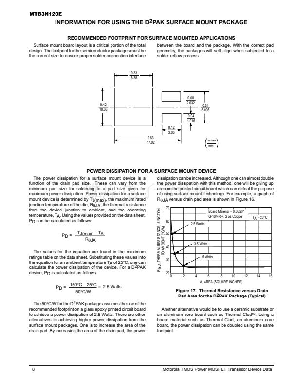
(1) When surface mounted to an FR4 board using the minimum recommended pad size.
E鈥揊ET and Designer鈥檚 are trademarks of Motorola, Inc.
TMOS is a registered trademark of Motorola, Inc.
Thermal Clad is a trademark of the Bergquist Company.
Preferred
devices are Motorola recommended choices for future use and best overall value.
REV 1
CASE 418B鈥?2, Style 2
D2PAK
Symbol
VDSS
VDGR
VGS
VGSM
ID
ID
IDM
PD
Value
1200
1200
20
40
3.0
2.2
11
125
1.0
2.5
鈥?55 to 150
101
1.0
62.5
50
260
Unit
Vdc
Vdc
Vdc
Vpk
Adc
Apk
Watts
W/擄C
Watts
擄C
mJ
擄C/W
TJ, Tstg
EAS
R
胃JC
R
胃JA
R
胃JA
TL
擄C
Motorola, Inc. 1995
Motorola TMOS Power MOSFET Transistor Device Data
1

MTB3N120E相關型號PDF文件下載

掃碼下載APP,
一鍵連接廣大的電子世界。

在線人工客服

買家服務:
賣家服務:
技術客服:

0571-85317607

網(wǎng)站技術支持

13606545031

客服在線時間周一至周五
9:00-17:30

關注官方微信號,
第一時間獲取資訊。

建議反饋

聯(lián)系人:

聯(lián)系方式:

按住滑塊,拖拽到最右邊
>>
感謝您向阿庫提出的寶貴意見,您的參與是維庫提升服務的動力!意見一經(jīng)采納,將有感恩紅包奉上哦!