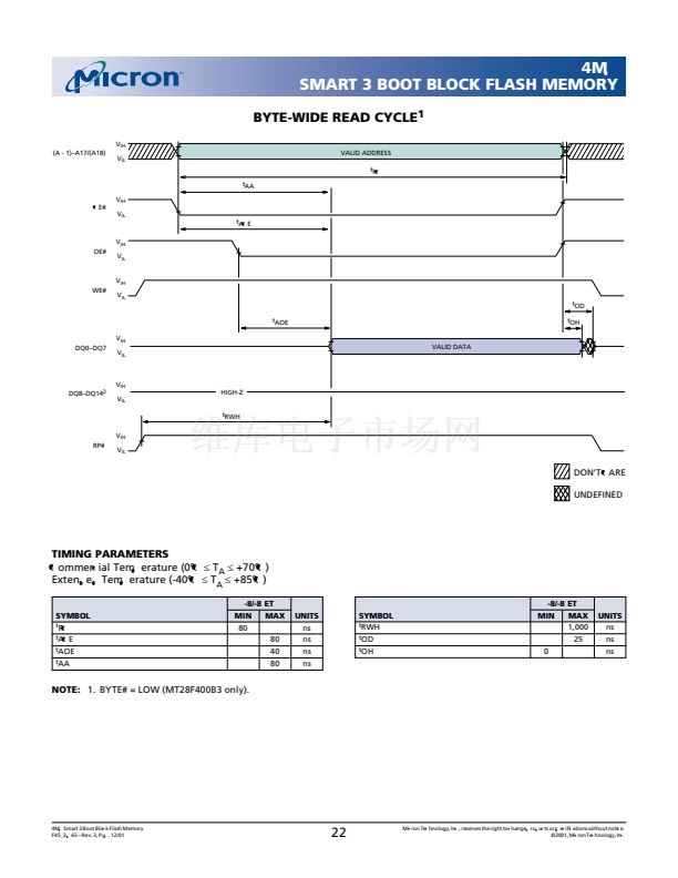
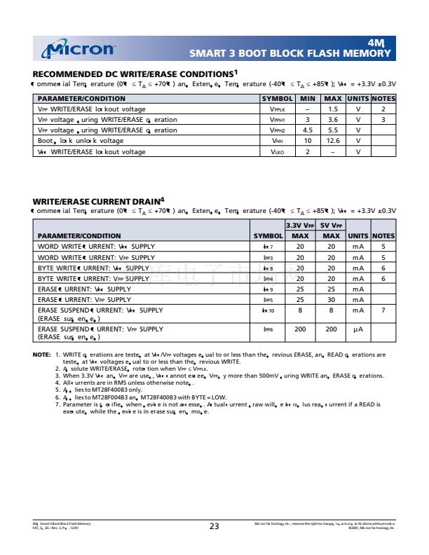
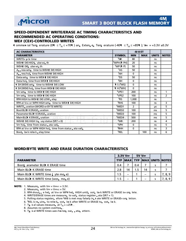
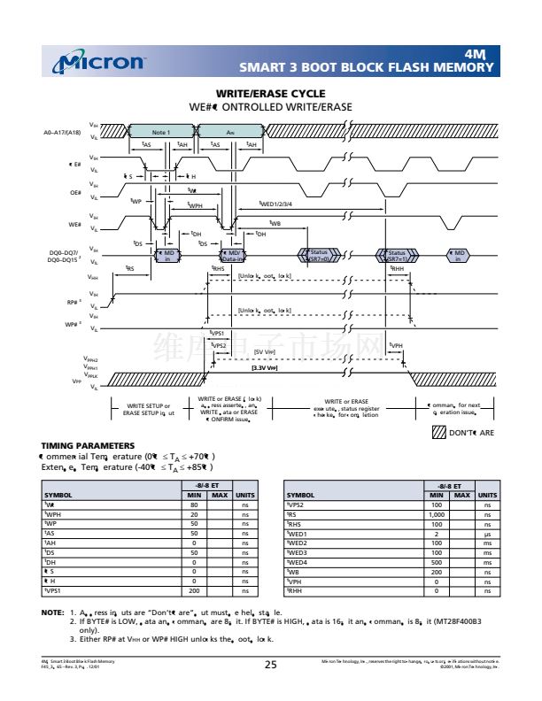
4Mb
SMART 3 BOOT BLOCK FLASH MEMORY
FLASH MEMORY
MT28F004B3
MT28F400B3
3V Only, Dual Supply (Smart 3)
FEATURES
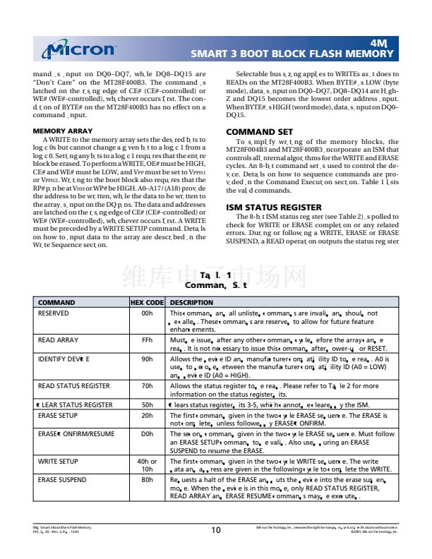
鈥?Seven erase blocks:
16KB/8K-word boot block (protected)
Two 8KB/4K-word parameter blocks
Four main memory blocks
鈥?Smart 3 technology (B3):
3.3V 鹵0.3V V
CC
3.3V 鹵0.3V V
PP
application programming
5V 鹵10% V
PP
application/production programming
1
鈥?Compatible with 0.3碌m Smart 3 device
鈥?Advanced 0.18碌m CMOS floating-gate process
鈥?Address access time: 80ns
鈥?100,000 ERASE cycles
鈥?Industry-standard pinouts
鈥?Inputs and outputs are fully TTL-compatible
鈥?Automated write and erase algorithm
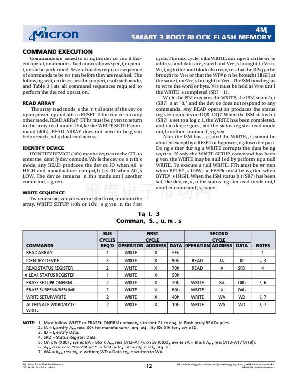
鈥?Two-cycle WRITE/ERASE sequence
鈥?Byte- or word-wide READ and WRITE
(MT28F400B3, 256K x 16/512K x 8)
鈥?Byte-wide READ and WRITE only
(MT28F004B3, 512K x 8)
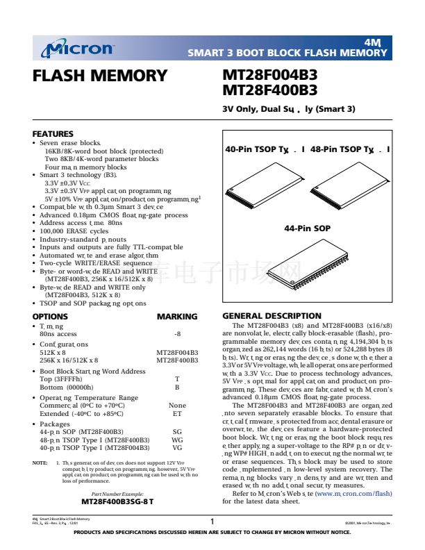
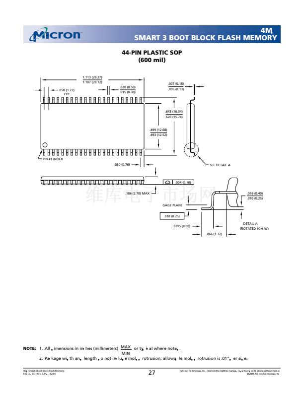
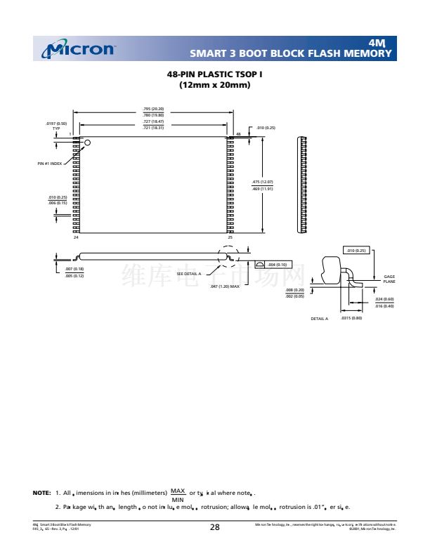
鈥?TSOP and SOP packaging options
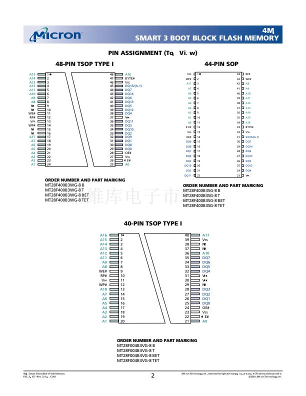
40-Pin TSOP Type I 48-Pin TSOP Type I
44-Pin SOP
OPTIONS
鈥?Timing
80ns access
鈥?Configurations
512K x 8
256K x 16/512K x 8
鈥?Boot Block Starting Word Address
Top (3FFFFh)
Bottom (00000h)
鈥?Operating Temperature Range
Commercial (0潞C to +70潞C)
Extended (-40潞C to +85潞C)
鈥?Packages
44-pin SOP (MT28F400B3)
48-pin TSOP Type I (MT28F400B3)
40-pin TSOP Type I (MT28F004B3)
NOTE:
MARKING
-8
MT28F004B3
MT28F400B3
T
B
None
ET
SG
WG
VG
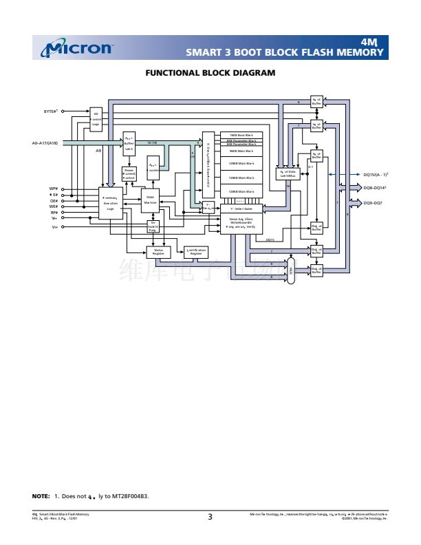
GENERAL DESCRIPTION
The MT28F004B3 (x8) and MT28F400B3 (x16/x8)
are nonvolatile, electrically block-erasable (flash), pro-
grammable memory devices containing 4,194,304 bits
organized as 262,144 words (16 bits) or 524,288 bytes (8
bits). Writing or erasing the device is done with either a
3.3V or 5V V
PP
voltage, while all operations are performed
with a 3.3V V
CC
. Due to process technology advances,
5V V
PP
is optimal for application and production pro-
gramming. These devices are fabricated with Micron鈥檚
advanced 0.18碌m CMOS floating-gate process.
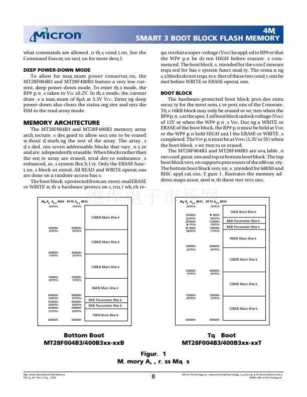
The MT28F004B3 and MT28F400B3 are organized
into seven separately erasable blocks. To ensure that
critical firmware is protected from accidental erasure or
overwrite, the devices feature a hardware-protected
boot block. Writing or erasing the boot block requires
either applying a super-voltage to the RP# pin or driv-
ing WP# HIGH in addition to executing the normal write
or erase sequences. This block may be used to store
code implemented in low-level system recovery. The
remaining blocks vary in density and are written and
erased with no additional security measures.
Refer to Micron鈥檚 Web site (www.micron.com/flash)
for the latest data sheet.
1. This generation of devices does not support 12V V
PP
compatibility production programming; however, 5V V
PP
application production programming can be used with no
loss of performance.
Part Number Example:
MT28F400B3SG-8 T
4Mb Smart 3 Boot Block Flash Memory
F45_3.p65 鈥?Rev. 3, Pub. 12/01
1
漏2001, Micron Technology, Inc.
PRODUCTS AND SPECIFICATIONS DISCUSSED HEREIN ARE SUBJECT TO CHANGE BY MICRON WITHOUT NOTICE.


 1
1
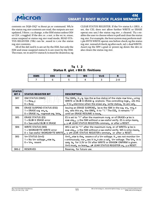
 2
2
 3
3
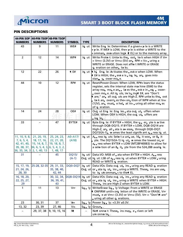 4
4
 5
5
 6
6
 7
7
 8
8
 9
9
 10
10
 11
11
 12
12
 13
13
 14
14
 15
15
 16
16
 17
17
 18
18
 19
19
 20
20
 21
21
 22
22
 23
23
 24
24
 25
25
 26
26
 27
27
 28
28
 29
29
 30
30
