鈮?/div>
10
碌s)
Source Current 鈥?Continuous @ TA = 25擄C
Total Power Dissipation @ TA = 25擄C (1)
Operating and Storage Temperature Range
Single Pulse Drain鈥搕o鈥揝ource Avalanche Energy 鈥?STARTING TJ = 25擄C
(VDD = 30 Vdc, VGS = 5.0 Vdc, VDS = 32 Vdc, IL = 10 Apk, L = 10 mH, RG = 25
W
)
Thermal Resistance 鈥?Junction鈥搕o鈥揂mbient
Maximum Temperature for Soldering
Symbol
VDSS
VGS
ID
IDM
IS
PD
TJ, Tstg
EAS
R
胃JA
T
Value
30
鹵
20
7.0
50
2.3
2.5
鈥?55 to 150
5000
50
260
Unit
Vdc
Vdc
Adc
Apk
Adc
Watts
擄C
mJ
擄C/W
擄C
DEVICE MARKING
S7P03
(1) When mounted on 1 inch square FR鈥? or G鈥?0 (VGS = 10 V @ 10 seconds)
ORDERING INFORMATION
Device
MMSF7P03HDR2
Reel Size
13鈥?/div>
Tape Width
12 mm embossed tape
Quantity
2500 units
Designer鈥檚 Data for 鈥淲orst Case鈥?Conditions
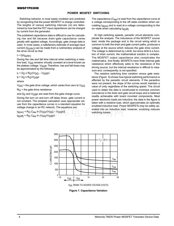
鈥?The Designer鈥檚 Data Sheet permits the design of most circuits entirely from the information presented. SOA Limit
curves 鈥?representing boundaries on device characteristics 鈥?are given to facilitate 鈥渨orst case鈥?design.
Preferred devices
are Motorola recommended choices for future use and best overall value.
Designer鈥檚 and HDTMOS are trademarks of Motorola, Inc. TMOS is a registered trademark of Motorola, Inc.
Thermal Clad is a trademark of the Bergquist Company.
REV 2
漏
Motorola TMOS Power MOSFET Transistor Device Data
Motorola, Inc. 1997
1


 1
1
 2
2
 3
3
 4
4
 5
5
 6
6
 7
7
 8
8
 9
9
 10
10
